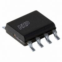
PCA9600D,112 NXP Semiconductors, PCA9600D,112 Datasheet - Page 6

PCA9600D,112
Manufacturer Part Number
PCA9600D,112
Description
IC DUAL BI-DIR BUS BUFFER 8-SOIC
Manufacturer
NXP Semiconductors
Type
Bufferr
Datasheet
1.PCA9600D112.pdf
(31 pages)
Specifications of PCA9600D,112
Package / Case
8-SOIC (3.9mm Width)
Mounting Type
Surface Mount
Current - Supply
7.3mA
Voltage - Supply
2.5 V ~ 15 V
Delay Time
100ns
Capacitance - Input
10pF
Tx/rx Type
I²C Logic
Supply Voltage (max)
15 V
Supply Voltage (min)
2.5 V
Maximum Operating Temperature
+ 85 C
Mounting Style
SMD/SMT
Minimum Operating Temperature
- 40 C
Lead Free Status / RoHS Status
Lead free / RoHS Compliant
Other names
935285243112::PCA9600D::PCA9600D
NXP Semiconductors
8. Limiting values
PCA9600
Product data sheet
When the device driving the PCA9600 is an I
PCA9600 is an improvement on the P82B96 as shown in
exceptions however, and if the device driving the bus buffer is not I
(e.g., you need to use the micro already in the system and bit-bang using two GPIO pins)
then here are some considerations that would point to using the P82B96 instead:
Table 5.
In accordance with the Absolute Maximum Rating System (IEC 60134).
Voltages with respect to pin GND.
[1]
Symbol
V
V
V
V
I
P
T
T
T
I2C-bus
•
•
•
j
stg
amb
CC
I2C-bus
O
I
tot
When the pull-up must be the weakest one possible. The spec is 200 μA for P82B96,
but it typically works even below that. And if designing for a temperature range −40 °C
up to +60 °C, then the driver when sinking 200 μA only needs to drive a guaranteed
low of 0.55 V. For the PCA9600, over that same temperature range and when sinking
1.3 mA (at −40 °C), the device driving the bus buffer must provide the required low of
0.425 V.
When the lower operating temperature range is restricted (say 0 °C). The P82B96
larger SX voltage levels then make a better typical match with the driver, even when
the supply is as low as 3.3 V.
For an I
low that is below 0.83 V. P82B96 guarantees that with a 200 μA pull-up.
When the operating temperature range is restricted at both limits. An I
typical output is well below 0.4 V and the P82B96 typically requires 0.6 V input even
at +60 °C, so there is a reasonable margin. The PCA9600 requires a typical input low
of 0.5 V so its typical margin is smaller. At 0 °C the driver requires a typical input low
of 1.16 V and P82B96 provides 0.75 V, so again the typical margin is already quite big
and even though PCA9600 is better, providing 0.7 V, that difference is not big.
See also
Limiting values
Section 10.2 “Negative undershoot below absolute minimum
Parameter
supply voltage
I
output voltage
input voltage
I
total power dissipation
junction temperature
storage temperature
ambient temperature
2
2
2
C-bus compliant driver on 3.3 V the P82B96 is required to guarantee a bus
C-bus voltage
C-bus current
All information provided in this document is subject to legal disclaimers.
Rev. 5 — 5 May 2011
Conditions
V
SX and SY;
I
TX and TY;
buffered output
RX and RY;
receive input
SX and SY;
I
operating range
operating
2
2
CC
C-bus SDA or SCL
C-bus SDA or SCL
to GND
2
C-bus compatible device, then the
Table
Dual bidirectional bus buffer
value”.
[1]
[1]
4. There will always be
Min
−0.3
−0.3
−0.3
−0.3
-
-
−40
−55
−40
2
C-bus compatible
PCA9600
© NXP B.V. 2011. All rights reserved.
Max
+18
+18
+18
+18
250
300
+125
+125
+85
2
C driver's
Unit
V
V
V
V
mA
mW
°C
°C
°C
6 of 31


