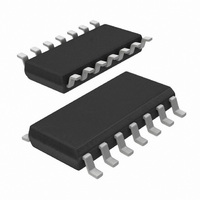
PCA9543AD,118 NXP Semiconductors, PCA9543AD,118 Datasheet - Page 9

PCA9543AD,118
Manufacturer Part Number
PCA9543AD,118
Description
IC I2C SWITCH 2CH 14-SOIC
Manufacturer
NXP Semiconductors
Datasheet
1.PCA9543APW118.pdf
(23 pages)
Specifications of PCA9543AD,118
Applications
2-Channel I²C Multiplexer
Interface
I²C, SMBus
Voltage - Supply
2.3 V ~ 5.5 V
Package / Case
14-SOIC (3.9mm Width), 14-SOL
Mounting Type
Surface Mount
For Use With
OM6285 - EVAL BOARD I2C-2002-1A568-4002 - DEMO BOARD I2C568-3615 - DEMO BOARD I2C
Lead Free Status / RoHS Status
Lead free / RoHS Compliant
Other names
568-1857-2
935275803118
PCA9543AD-T
935275803118
PCA9543AD-T
NXP Semiconductors
PCA9543A_43B_43C_6
Product data sheet
Fig 11. System configuration
SDA
SCL
TRANSMITTER/
RECEIVER
MASTER
7.3 System configuration
7.4 Acknowledge
A device generating a message is a ‘transmitter’, a device receiving is the ‘receiver’. The
device that controls the message is the ‘master’ and the devices which are controlled by
the master are the ‘slaves’ (see
The number of data bytes transferred between the START and the STOP conditions from
transmitter to receiver is not limited. Each byte of eight bits is followed by one
acknowledge bit. The acknowledge bit is a HIGH level put on the bus by the transmitter,
whereas the master generates an extra acknowledge related clock pulse.
A slave receiver which is addressed must generate an acknowledge after the reception of
each byte. Also, a master must generate an acknowledge after the reception of each byte
that has been clocked out of the slave transmitter. The device that acknowledges has to
pull down the SDA line during the acknowledge clock pulse, so that the SDA line is stable
LOW during the HIGH period of the acknowledge related clock pulse; set-up and hold
times must be taken into account.
A master receiver must signal an end of data to the transmitter by not generating an
acknowledge on the last byte that has been clocked out of the slave. In this event, the
transmitter must leave the data line HIGH to enable the master to generate a STOP
condition.
Fig 12. Acknowledgement on the I
RECEIVER
SLAVE
SCL from master
by transmitter
data output
by receiver
data output
TRANSMITTER/
Rev. 06 — 15 June 2009
RECEIVER
condition
START
SLAVE
S
2-channel I
Figure
2
C-bus
TRANSMITTER
1
11).
MASTER
2
C-bus switch with interrupt logic and reset
PCA9543A/43B/43C
2
TRANSMITTER/
RECEIVER
MASTER
acknowledgement
not acknowledge
SLAVE
clock pulse for
acknowledge
8
MULTIPLEXER
© NXP B.V. 2009. All rights reserved.
002aaa987
I
2
9
C-BUS
002aaa966
9 of 23


