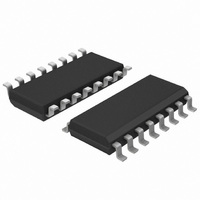
UJA1023T/2R04,512 NXP Semiconductors, UJA1023T/2R04,512 Datasheet - Page 28

UJA1023T/2R04,512
Manufacturer Part Number
UJA1023T/2R04,512
Description
IC CAN/LIN I/O SLAVE 32HTSSOP
Manufacturer
NXP Semiconductors
Datasheet
1.UJA1023T2R04C51.pdf
(49 pages)
Specifications of UJA1023T/2R04,512
Applications
LIN Controller
Interface
LIN (Local Interconnect Network)
Voltage - Supply
6.5 V ~ 27 V
Package / Case
16-SOIC (3.9mm Width)
Mounting Type
Surface Mount
Lead Free Status / RoHS Status
Lead free / RoHS Compliant
Other names
935281302512
UJA1023T/2R04
UJA1023T/2R04
UJA1023T/2R04
UJA1023T/2R04
NXP Semiconductors
UJA1023
Product data sheet
7.2.3.6 ADC mode
This means that the scan matrix value is determined directly after the previous LIN
message.
In case two or more switches are closed simultaneously, extra diodes have to be added to
prevent the ‘short-circuit’ of neighbor switches.
For the switch matrix inputs a ‘quasi’ capture mode can be configured via the data bit
SMC (D3.3) of the second configuration block. If a matrix switch input value has been
changed the changed value is captured until the master reads the switch matrix value via
the UJA1023 command PxResp. Note that two readings are necessary for proper
initialization.
A switch matrix can be configured as local wake-up. If the data bit SMW (D3.2) of the
second configuration block is set to logic 1, a change of a matrix switch input value
causes a wake-up of the UJA1023. If in addition the Switch matrix capture mode is
enabled via SMC the switch matrix value of PxResp represents the local wake-up source
switch of the switch matrix.
The principle of the bit stream ADC is shown in
are needed per analog input, which should be dimensioned as: R
C1 = 10 nF. All eight inputs can be used as analog input, one at a time. ADC values are
referenced to V
of the bit stream. This ratio represents the analog voltage V
to define the measurement period, typically 1.5 ms.
Fig 8.
Switch matrix principle
V
V
V
V
th1
th1
th1
th1
VIO
All information provided in this document is subject to legal disclaimers.
. A register/counter is used to count the ratio of HIGH and LOW phases
Rev. 5 — 17 August 2010
R
1 kΩ
R
1 kΩ
R
1 kΩ
R
1 kΩ
on(HS)
on(HS)
on(HS)
on(HS)
P0
P1
P2
P3
P4
R
50 Ω
on(LS)
SM40
SM41
Figure
P5
R
50 Ω
on(LS)
9. Only three external components
A
. The upper counter is used
P6
R
50 Ω
i
on(LS)
= R1 = 100 kΩ;
UJA1023
© NXP B.V. 2010. All rights reserved.
LIN-I/O slave
P7
R
50 Ω
on(LS)
mdb496
SM72
SM73
28 of 49


