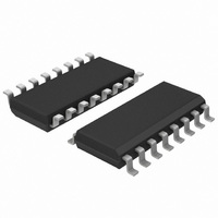
UJA1023T/2R04,512 NXP Semiconductors, UJA1023T/2R04,512 Datasheet - Page 31

UJA1023T/2R04,512
Manufacturer Part Number
UJA1023T/2R04,512
Description
IC CAN/LIN I/O SLAVE 32HTSSOP
Manufacturer
NXP Semiconductors
Datasheet
1.UJA1023T2R04C51.pdf
(49 pages)
Specifications of UJA1023T/2R04,512
Applications
LIN Controller
Interface
LIN (Local Interconnect Network)
Voltage - Supply
6.5 V ~ 27 V
Package / Case
16-SOIC (3.9mm Width)
Mounting Type
Surface Mount
Lead Free Status / RoHS Status
Lead free / RoHS Compliant
Other names
935281302512
UJA1023T/2R04
UJA1023T/2R04
UJA1023T/2R04
UJA1023T/2R04
NXP Semiconductors
UJA1023
Product data sheet
Table 27.
Table 28.
[1]
Data byte
D0
D1
D2
D3
Byte
D0
Bytes D1 and D2 if switch matrix is not configured (default)
D1
D2
Bytes D1 and D2 if switch matrix is configured
D1
D2
Byte D3
D3
Data bytes D2 and D3 are transmitted only if bit TxDL = 1 (bit 4 of byte D3 in the second I/O configuration
data block, see
[1]
Bit
7 to 0
7 to 0
7 to 0
7 to 0
7 to 0
7 to 0
7 to 0
PxResp frame bit allocation
PxResp frame bit allocation
7
P7
EC7
SM53
PxL7
SM73
PWM7
ADC7
All information provided in this document is subject to legal disclaimers.
Table 17
Symbol
P[7:0]
EC[7:0]
PxL[7:0]
SMxx
SMxx
PWM[7:0]
ADC[7:0]
6
P6
EC6
SM52
PxL6
SM72
PWM6
ADC6
Rev. 5 — 17 August 2010
and
Table
5
P5
EC5
SM51
PxL5
SM71
PWM5
ADC5
Description
Px input value.
Edge capture value.
PxOut latch value.
Switch matrix value 0. Refer to
Switch matrix value 1.
PWM value.
ADC value. The ADC value is transmitted only if the INH output
is in ADC mode (IM0 = 1, IM1 = 0).
18).
4
P4
EC4
SM50
PxL4
SM70
PWM4
ADC4
[1]
3
P3
EC3
SM43
PxL3
SM63
PWM3
ADC3
[1]
Figure
2
P2
EC2
SM42
PxL2
SM62
PWM2
ADC2
8.
UJA1023
1
P1
EC1
SM41
PxL1
SM61
PWM1
ADC1
© NXP B.V. 2010. All rights reserved.
LIN-I/O slave
0
P0
EC0
SM40
PxL0
SM60
PWM0
ADC0
31 of 49


