ISL8499IRZ Intersil, ISL8499IRZ Datasheet
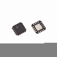
IC SWITCH QUAD SPDT 16QFN

ISL8499IRZ

Manufacturer Part Number
ISL8499IRZ
Description
IC SWITCH QUAD SPDT 16QFN
Manufacturer
Intersil
Datasheet

Specifications of ISL8499IRZ

Function
Switch
Circuit
4 x SPDT
On-state Resistance
250 mOhm
Voltage Supply Source
Single Supply
Voltage - Supply, Single/dual (±)
1.65 V ~ 4.5 V
Current - Supply
0.09µA
Operating Temperature
-40°C ~ 85°C
Mounting Type
Surface Mount
Package / Case
16-VQFN Exposed Pad, 16-HVQFN, 16-SQFN, 16-DHVQFN
Rohs Compliant
YES
Lead Free Status / RoHS Status
Lead free / RoHS Compliant

Available stocks

Company
Part Number
Manufacturer
Quantity
Price
Part Number:
ISL8499IRZ
Manufacturer:
INTERSIL
Quantity:
31 959
Part Number:
ISL8499IRZ-T
Manufacturer:
INTERSIL
Quantity:
24 000
Ultra Low ON-Resistance, +1.65V to +4.5V,
Single Supply, Quad SPDT (Dual DPDT)
Analog Switch
The Intersil ISL8499 device is a low ON-Resistance, low
voltage, bidirectional, Quad SPDT (Dual DPDT) analog
switch designed to operate from a single +1.65V to +4.5V
supply. Targeted applications include battery powered
equipment that benefit from low r
switching speeds (t
input is 1.8V logic-compatible when using a single +3V supply.
With a supply voltage of 4.2V and logic high voltage of 2.85V
at both logic inputs, the part draws only 10µA max of ICC
current.
Cell phones, for example, often face ASIC functionality
limitations. The number of analog input or GPIO pins may be
limited and digital geometries are not well suited to analog
switch performance. This part may be used to “mux-in”
additional functionality while reducing ASIC design risk. The
ISL8499 is offered in small form factor packages, alleviating
board space limitations.
The ISL8499 consists of four SPDT switches. It is configured
as a dual double-pole/double-throw (DPDT) device with two
logic control inputs that control two SPDT switches each. The
configuration can be used as a dual differential 2-to-1
multiplexer/demultiplexer. The ISL8499 is pin compatible with
the STG3699 and DG2799.
Number of Switches
4.3V t
3.0V t
1.8V t
Packages
4.3V
3.0V
1.8V
SW
ON
ON
ON
TABLE 1. FEATURES AT A GLANCE
-
r
r
r
ON
ON
ON
/t
/t
/t
OFF
OFF
OFF
ON
= 15ns, t
®
16 Ld 3x3 TQFN, 16 Ld 3x3 QFN,
1
OFF
Quad SPDT (Dual DPDT)
ON
(0.24Ω) and fast
= 13ns). The digital logic
Data Sheet
16 Ld TSSOP
15ns/13ns
21ns/17ns
51ns/43ns
ISL8499
0.24Ω
0.26Ω
0.45Ω
4
1-888-INTERSIL or 1-888-468-3774
CAUTION: These devices are sensitive to electrostatic discharge; follow proper IC Handling Procedures.
Features
• Drop in Replacement for the STG3699 and DG2799
• ON-Resistance (
• Single Supply Operation . . . . . . . . . . . . . . . +1.65V to +4.5V
• Low Power Consumption (PD) . . . . . . . . . . . . . . . . . <0.2µW
• Fast Switching Action (V+ = +4.3V)
• Guaranteed Break-Before-Make
• 1.8V Logic Compatible (+3V supply)
• Low ICC Current when VinH is not at the V+ Rail
• Available in 16 Ld 3x3 TQFN, 16 Ld 3x3 QFN and
• ESD HBM Rating
• Pb-Free Available (RoHS Compliant)
Applications
• Battery Powered, Handheld, and Portable Equipment
• Portable Test and Measurement
• Medical Equipment
• Audio and Video Switching
Related Literature
• Technical Brief TB363 “Guidelines for Handling and
• Application Note AN557 “Recommended Test Procedures
- V+ = +4.3V . . . . . . . . . . . . . . . . . . . . . . . . . . . . . . 0.24Ω
- V+ = +3.0V . . . . . . . . . . . . . . . . . . . . . . . . . . . . . . 0.26Ω
- V+ = +1.8V . . . . . . . . . . . . . . . . . . . . . . . . . . . . . . 0.45Ω
r
r
- t
- t
16 Ld TSSOP
- COM Pins. . . . . . . . . . . . . . . . . . . . . . . . . . . . . . . . . 9kV
- All Other Pins . . . . . . . . . . . . . . . . . . . . . . . . . . . . . . 4kV
- Cellular/Mobile Phones
- Pagers
- Laptops, Notebooks, Palmtops
Processing Moisture Sensitive Surface Mount Devices
(SMDs)”
for Analog Switches”
ON
ON
February 5, 2008
ON
OFF
Matching between Channels . . . . . . . . . . . . . . . . . 0.04Ω
Flatness Across Signal Range . . . . . . . . . . . . . . . 0.05Ω
All other trademarks mentioned are the property of their respective owners.
. . . . . . . . . . . . . . . . . . . . . . . . . . . . . . . . . . . . . 15ns
. . . . . . . . . . . . . . . . . . . . . . . . . . . . . . . . . . . . 13ns
|
Copyright Intersil Americas Inc. 2005-2006, 2008. All Rights Reserved
Intersil (and design) is a registered trademark of Intersil Americas Inc.
r
ON
)
ISL8499
FN6111.3

Related parts for ISL8499IRZ

ISL8499IRZ Summary of contents

Page 1

... CAUTION: These devices are sensitive to electrostatic discharge; follow proper IC Handling Procedures. 1-888-INTERSIL or 1-888-468-3774 All other trademarks mentioned are the property of their respective owners. ISL8499 FN6111 15ns . . . . . . . . . . . . . . . . . . . . . . . . . . . . . . . . . . . . 13ns | Intersil (and design registered trademark of Intersil Americas Inc. Copyright Intersil Americas Inc. 2005-2006, 2008. All Rights Reserved ...

Page 2

... Analog Switch Normally Closed Pin 2 ISL8499 Ordering Information PART NUMBER ISL8499IR V+ ISL8499IR-T* NC4 COM4 ISL8499IV NO4 ISL8499IV-T* IN3-4 NC3 ISL8499IRZ COM3 (Note) NO3 ISL8499IRZ-T* (Note) ISL8499IVZ (Note) ISL8499IVZ-T* (Note) ISL8499IRTZ (Note) 12 COM4 ISL8499IRTZ-T* (Note) NO4 11 IN3-4 10 *Please refer to TB347 for details on reel specifications NC3 9 NOTE: These Intersil Pb-free plastic packaged products employ special Pb-free material sets ...

Page 3

... TQFN and QFN Package (Notes TSSOP Package (Note Maximum Junction Temperature (Plastic Package +150°C Maximum Storage Temperature Range . . . . . . . . . . . -65°C to +150°C Pb-Free Reflow Profile .see link below http://www.intersil.com/pbfree/Pb-FreeReflow.asp Operating Conditions Temperature Range ISL8499IX . . . . . . . . . . . . . . . . . . . . . . . . . . . . . . . . -40°C to +85°C Test Conditions +3.9V to +4.5V, GND = 0V, V ...

Page 4

Electrical Specifications - 4.3V Supply PARAMETER Total Harmonic Distortion f = 20Hz to 20kHz OFF Capacitance 1MHz, V OFF COM ON Capacitance 1MHz, V COM(ON) POWER SUPPLY CHARACTERISTICS Power Supply ...

Page 5

Electrical Specifications - 3V Supply PARAMETER Charge Injection 1.0nF OFF Isolation R = 50Ω (See Figure 4) Crosstalk (Channel-to-Channel 50Ω (See Figure 6) Total Harmonic Distortion f = 20Hz ...

Page 6

Test Circuits and Waveforms V+ LOGIC 50% INPUT 0V t OFF SWITCH V NO INPUT V 90% SWITCH OUTPUT Logic input waveform is inverted for switches that have the opposite logic sense. FIGURE 1A. MEASUREMENT POINTS SWITCH ...

Page 7

Test Circuits and Waveforms SIGNAL GENERATOR COM ANALYZER GND R L FIGURE 4. OFF ISOLATION TEST CIRCUIT SIGNAL GENERATOR COM ANALYZER GND R L FIGURE 6. ...

Page 8

above GND. The low leakage current performance is unaffected by this approach, but the switch signal range is reduced and the resistance may increase, especially at low supply ...

Page 9

Typical Performance Curves 0.45 0. 1.8V 0.35 0. 2. 3.6V 0. (V) COM FIGURE 9. ON-RESISTANCE vs SUPPLY VOLTAGE vs SWITCH VOLTAGE 0.35 0.30 +85°C ...

Page 10

Typical Performance Curves 200 150 100 +85°C +25°C -40° 1.5 2.0 2.5 3.0 V+ (V) FIGURE 15. TURN - ON TIME vs SUPPLY VOLTAGE GAIN -20 PHASE R = 50Ω ...

Page 11

Typical Performance Curves 200 Sweeping Both Logic Inputs 150 100 (V) IN1-4 FIGURE 21. SUPPLY CURRENT vs VLOGIC 11 ISL8499 T = +25°C, Unless Otherwise Specified (Continued) A Die Characteristics V+ = 4.2V SUBSTRATE POTENTIAL ...

Page 12

Thin Shrink Small Outline Plastic Packages (TSSOP) N INDEX 0.25(0.010) E AREA E1 - 0.05(0.002) SEATING PLANE - -C- α 0.10(0.004) 0.10(0.004 NOTES: 1. These package ...

Page 13

Package Outline Drawing L16.3x3 16 LEAD QUAD FLAT NO-LEAD PLASTIC PACKAGE Rev 2, 4/07 3.00 6 PIN 1 INDEX AREA (4X) 0.15 TOP VIEW ( 2. 80 TYP ) ( TYPICAL RECOMMENDED LAND PATTERN 13 ISL8499 A ...

Page 14

... Accordingly, the reader is cautioned to verify that data sheets are current before placing orders. Information furnished by Intersil is believed to be accurate and reliable. However, no responsibility is assumed by Intersil or its subsidiaries for its use; nor for any infringements of patents or other rights of third parties which may result from its use ...

Related keywords