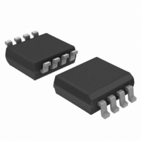
74LVC2G66DC,125 NXP Semiconductors, 74LVC2G66DC,125 Datasheet - Page 10

74LVC2G66DC,125
Manufacturer Part Number
74LVC2G66DC,125
Description
IC SWITCH DUAL SPST 8VSSOP
Manufacturer
NXP Semiconductors
Series
74LVCr
Type
Analog Switchr
Datasheet
1.74LVC2G66GM125.pdf
(26 pages)
Specifications of 74LVC2G66DC,125
Package / Case
8-VFSOP (0.091", 2.3mm Width)
Function
Switch
Circuit
2 x SPST - NO
On-state Resistance
6 Ohm
Voltage Supply Source
Single Supply
Voltage - Supply, Single/dual (±)
1.65 V ~ 5.5 V
Current - Supply
0.1µA
Operating Temperature
-40°C ~ 125°C
Mounting Type
Surface Mount
Switch Configuration
SPST
On Resistance (max)
34 Ohm (Typ) @ 1.95 V
On Time (max)
4.6 ns (Typ) @ 1.95 V
Off Time (max)
3.8 ns (Typ) @ 1.95 V
Supply Voltage (max)
5.5 V
Supply Voltage (min)
1.65 V
Maximum Power Dissipation
250 mW
Maximum Operating Temperature
+ 125 C
Mounting Style
SMD/SMT
Minimum Operating Temperature
- 40 C
Switch Current (typ)
0.0001 mA @ 5.5 V
Package
8VSSOP
Maximum On Resistance
195@1.95V Ohm
Maximum Propagation Delay Bus To Bus
0.8(Typ)@1.95V|0.4(Typ)@2.7V|0.3(Typ)@3.6V|0.2(Typ)@5.5V ns
Maximum Low Level Output Current
50 mA
Maximum Turn-off Time
3.8(Typ)@1.95V ns
Maximum Turn-on Time
4.6(Typ)@1.95V ns
Switch Architecture
SPST
Power Supply Type
Single
Lead Free Status / RoHS Status
Lead free / RoHS Compliant
Lead Free Status / RoHS Status
Lead free / RoHS Compliant, Lead free / RoHS Compliant
Other names
74LVC2G66DC-G
74LVC2G66DC-G
935274429125
74LVC2G66DC-G
935274429125
NXP Semiconductors
11. Dynamic characteristics
Table 9.
At recommended operating conditions; voltages are referenced to GND (ground = 0 V); for test circuit see
[1]
[2]
[3]
[4]
[5]
[6]
74LVC2G66
Product data sheet
Symbol Parameter
t
t
t
C
pd
en
dis
PD
Typical values are measured at T
t
Propagation delay is the calculated RC time constant of the typical ON resistance of the switch and the specified capacitance when
driven by an ideal voltage source (zero output impedance).
t
t
C
P
f
f
C
C
V
N = number of inputs switching;
pd
en
dis
i
o
PD
D
= input frequency in MHz;
L
S(ON)
CC
= output frequency in MHz;
is the same as t
is the same as t
= output load capacitance in pF;
is the same as t
= C
is used to determine the dynamic power dissipation (P
= supply voltage in V;
propagation delay nY to nZ or nZ to nY;
enable time
disable time
power dissipation
capacitance
PD
= maximum ON-state switch capacitance in pF;
Dynamic characteristics
× V
CC
2
× f
PLH
PZH
PLZ
i
× N + Σ{(C
and t
and t
and t
PHL
PZL
PHZ
Conditions
see
nE to nY or nZ;
see
nE to nY or nZ; see
Figure 18
C
V
I
.
L
.
.
L
V
V
V
V
V
V
V
V
V
V
V
V
V
V
V
V
V
V
= GND to V
+ C
= 50 pF; f
amb
CC
CC
CC
CC
CC
CC
CC
CC
CC
CC
CC
CC
CC
CC
CC
CC
CC
CC
Figure 17
Figure 18
S(ON)
= 1.65 V to 1.95 V
= 2.3 V to 2.7 V
= 2.7 V
= 3.0 V to 3.6 V
= 4.5 V to 5.5 V
= 1.65 V to 1.95 V
= 2.3 V to 2.7 V
= 2.7 V
= 3.0 V to 3.6 V
= 4.5 V to 5.5 V
= 1.65 V to 1.95 V
= 2.3 V to 2.7 V
= 2.7 V
= 3.0 V to 3.6 V
= 4.5 V to 5.5 V
= 2.5 V
= 3.3 V
= 5.0 V
= 25 °C and nominal V
) × V
All information provided in this document is subject to legal disclaimers.
i
= 10 MHz;
CC
CC
2
× f
o
Rev. 5 — 16 June 2010
} where:
D
CC
in μW).
.
[2][3]
[4]
[5]
[6]
−40 °C to +85 °C
Min
-
-
-
-
-
1.0
1.0
1.0
1.0
1.0
1.0
1.0
1.0
1.0
1.0
-
-
-
4.6
Typ
0.8
0.4
0.4
0.3
0.2
2.7
2.7
2.4
1.8
3.8
2.1
3.5
3.0
2.2
9.0
11.0
15.7
[1]
Max
2.0
1.2
1.0
0.8
0.6
10
5.6
5.0
4.4
3.9
9.0
5.5
6.5
6.0
5.0
-
-
-
−40 °C to +125 °C
Min
-
-
-
-
-
1.0
1.0
1.0
1.0
1.0
1.0
1.0
1.0
1.0
1.0
-
-
-
74LVC2G66
© NXP B.V. 2010. All rights reserved.
Max
2.0
1.5
1.5
1.0
13.0
7.5
6.5
6.0
5.0
11.5
7.0
8.5
8.0
6.5
-
-
-
3.0
Figure
Bilateral switch
19.
Unit
ns
ns
ns
ns
ns
ns
ns
ns
ns
ns
ns
ns
ns
ns
ns
pF
pF
pF
10 of 26


