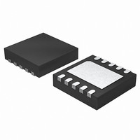
ISL54207IRZ-T Intersil, ISL54207IRZ-T Datasheet

ISL54207IRZ-T
Specifications of ISL54207IRZ-T
Related parts for ISL54207IRZ-T
ISL54207IRZ-T Summary of contents
Page 1
... GND CAUTION: These devices are sensitive to electrostatic discharge; follow proper IC Handling Procedures. | 1-888-INTERSIL or 1-888-468-3774 Intersil (and design registered trademark of Intersil Americas Inc. All other trademarks mentioned are the property of their respective owners. ISL54207 FN6403.0 Voltage on USB Cable ) . . . . . . . . . . . . 2.7V to 3.6V DD μ ...
Page 2
... PART (Note) MARKING ISL54207IRUZ-T FP ISL54207IRZ-T 207Z ISL54207IRZ 207Z NOTE: Intersil Pb-free plus anneal products employ special Pb-free material sets; molding compounds/die attach materials and 100% matte tin plate or NiPdAu termination finish, which are RoHS compliant and compatible with both SnPb and Pb-free soldering operations. Intersil Pb-free products are MSL classified at Pb-free peak reflow temperatures that meet or exceed the Pb-free requirements of IPC/JEDEC J STD-020 ...
Page 3
... Maximum Junction Temperature (Plastic Package +150°C DD Maximum Storage Temperature Range -65°C to +150° 0.3V) DD Operating Conditions Temperature Range ISL54207IRUZ and ISL54207IRZ -40°C to +85°C or GND by specified amount are clamped. Limit current to maximum current ratings. DD Test Conditions 1.4V, V CTRLH ...
Page 4
Electrical Specifications - 2.7V to 3.6V Supply PARAMETER OFF Leakage Current D+(OFF D-(OFF) NOx ON Leakage Current NOx DYNAMIC CHARACTERISTICS Turn-ON Time Turn-OFF Time, t ...
Page 5
Electrical Specifications - 2.7V to 3.6V Supply PARAMETER CTRL Voltage High CTRLH DD Input Current BUSL CTRLL DD Input Current BUSH DD Input Current CTRLH DD V Pull-Down Resistor, R ...
Page 6
Test Circuits and Waveforms V BUSH LOGIC INPUT V BUSL V OUT SWITCH OUTPUT 0V FIGURE 2A. MEASUREMENT POINTS /100mA ON 1 CTRL NCx V NCx V 1 100mA COMx GND Repeat test for all switches. FIGURE ...
Page 7
Test Circuits and Waveforms CTRL NCx or NOx IMPEDANCE ANALYZER COMx GND Repeat test for all switches. FIGURE 5. CAPACITANCE TEST CIRCUIT t ri 90% 50% 10% DIN+ t skew_i DIN- 90% 50% 10 90% 10% ...
Page 8
Application Block Diagram 22kΩ Detailed Description The ISL54207 device is a dual single pole/double throw (SPDT) analog switch device that operates from a single DC power supply in the range of 2.7V to 3.6V. It was designed to function as ...
Page 9
FIGURE 8. VECTOR-SCOPE PLOT BEFORE SWITCH FIGURE 9. VECTOR-SCOPE PLOT AFTER SWITCH Figure 18 shows the differential gain (DG) and differential phase (DP) plots at the output of the switch using an actual NTSC composite video signal and a VM700A ...
Page 10
USB Mode If the VBUS pin = Logic “1” and CTRL pin = Logic “0” or Logic “1,” the part will go into USB mode. In USB mode, the NO1 and NO2 5Ω switches are ON and the NC1 and ...
Page 11
Typical Performance Curves 0 32Ω LOAD FREQ = 1kHz 0.4 0.3 0.2 0 0.5 1.0 1.5 2.0 OUTPUT VOLTAGE (V FIGURE 12. THD+N vs OUTPUT VOLTAGE FIGURE 14. EYE PATTERN: 480Mbps WITH ...
Page 12
Typical Performance Curves 1 NOx SWITCH 50Ω 0. P-P P-P 1M 10M FREQUENCY (Hz) FIGURE 15. FREQUENCY RESPONSE 1 NCx SWITCHES ...
Page 13
... Maximum allowable burrs is 0.076mm in all directions. 9. Same as JEDEC MO-255UABD except: TERMINAL TIP No lead-pull-back, "A" MIN dimension = 0.45 not 0.50mm "L" MAX dimension = 0.45 not 0.42mm. 10. For additional information, to assist with the PCB Land Pattern Design effort, see Intersil Technical Brief TB389. L MILLIMETERS MIN NOMINAL MAX A 0 ...
Page 14
... Accordingly, the reader is cautioned to verify that data sheets are current before placing orders. Information furnished by Intersil is believed to be accurate and reliable. However, no responsibility is assumed by Intersil or its subsidiaries for its use; nor for any infringements of patents or other rights of third parties which may result from its use ...


