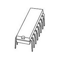
TEA1062A NXP Semiconductors, TEA1062A Datasheet - Page 12

TEA1062A
Manufacturer Part Number
TEA1062A
Description
Manufacturer
NXP Semiconductors
Datasheet
1.TEA1062A.pdf
(28 pages)
Specifications of TEA1062A
Primary Target Application
Telephone Sets
Operating Supply Voltage (typ)
2.7/3.4V
Max Transmitter Gain
53.5dB
Receiver Gain (max)
32.5dB
Operating Temp Range
-25C to 75C
Package Type
PDIP
Pin Count
16
Operating Current
900uA
Operating Temperature Classification
Commercial
Mounting
Through Hole
Operating Supply Voltage (min)
2.2V
Lead Free Status / Rohs Status
Compliant
Available stocks
Company
Part Number
Manufacturer
Quantity
Price
Company:
Part Number:
TEA1062A
Manufacturer:
UTC
Quantity:
4 119
Company:
Part Number:
TEA1062A
Manufacturer:
PHILIPS
Quantity:
4 043
Part Number:
TEA1062A
Manufacturer:
PHILIPS/飞利浦
Quantity:
20 000
Company:
Part Number:
TEA1062A*
Manufacturer:
LITEON
Quantity:
1
Company:
Part Number:
TEA1062A/UTC1062A
Manufacturer:
INTEL
Quantity:
1
Part Number:
TEA1062AN
Manufacturer:
UTC/友顺
Quantity:
20 000
Part Number:
TEA1062AT
Manufacturer:
HP
Quantity:
20 000
Philips Semiconductors
1997 Sep 03
SYMBOL
Gain adjustment inputs GAS1 and GAS2 (pins 2 and 3)
Sending amplifier output LN (pin 1)
V
V
Receiving amplifier input IR (pin 10)
Receiving amplifier output QR (pin 4)
G
V
V
V
Gain adjustment input GAR (pin 5)
Mute input (pin 12)
V
V
I
MUTE
Z
Z
G
G
G
G
LN(rms)
no(rms)
o(rms)
o(rms)
no(rms)
IH
IL
Low voltage transmission circuits with
dialler interface
v
i
o
v
vf
vT
v
transmitting amplifier gain variation by
adjustment of R7 between
GAS1 and GAS2
output voltage (RMS value)
noise output voltage (RMS value)
input impedance
output impedance
voltage gain from IR to QR
gain variation with frequency
referenced to 800 Hz
gain variation with temperature
referenced to 25 C
output voltage (RMS value)
output voltage (RMS value)
noise output voltage (RMS value)
receiving amplifier gain variation by
adjustment of R4 between GAR and QR
HIGH level input voltage
LOW level input voltage
input current
PARAMETER
THD = 10%
I
200
MIC+; psophometrically
weighted (P53 curve)
I
(from pin 9 to pin 4)
f = 300 and 3400 Hz
without R6; I
T
THD = 2%; sine wave drive;
R4 = 100 k ; I
I
THD = 10%; R4 = 100 k ;
R
I
IR open-circuit
psophometrically weighted
(P53 curve); R
line
line
p
line
amb
L
I
I
= 0 mA
R
R
line
line
= 150 ; I
= 15 mA; R7 = 68 k ;
= 15 mA; R
L
L
= 15 mA; R4 = 100 k ;
12
= 25 and +75 C
= 150
= 450
= 4 mA
= 15 mA
between MIC and
CONDITIONS
line
line
line
L
L
= 50 mA;
= 300
= 4 mA
= 300
= 15 mA;
TEA1062; TEA1062A
1.7
29.5
0.22
0.3
1.5
MIN.
8
11
0.8
2.3
21
4
31
0.33
0.48
15
50
8
TYP.
69
0.2
0.2
Product specification
0
32.5
0
V
0.3
15
MAX.
CC
dB
V
V
dBmp
k
dB
dB
dB
V
V
mV
dB
V
V
UNIT
V
A


