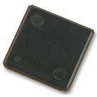
H5PS1G83EFR-S6C HYNIX SEMICONDUCTOR, H5PS1G83EFR-S6C Datasheet - Page 26

H5PS1G83EFR-S6C
Manufacturer Part Number
H5PS1G83EFR-S6C
Description
58T1895
Manufacturer
HYNIX SEMICONDUCTOR
Datasheet
1.H5PS1G83EFR-S6C.pdf
(44 pages)
Specifications of H5PS1G83EFR-S6C
Memory Type
SDRAM
Memory Configuration
128M X 8
Access Time
15ns
Memory Case Style
FBGA
No. Of Pins
60
Operating Temperature Range
0°C To +85°C
Memory Size
1 Gbit
Rohs Compliant
Yes
Available stocks
Company
Part Number
Manufacturer
Quantity
Price
Company:
Part Number:
H5PS1G83EFR-S6C
Manufacturer:
HYNIX
Quantity:
4 000
Part Number:
H5PS1G83EFR-S6C
Manufacturer:
HYNIX/海力士
Quantity:
20 000
Company:
Part Number:
H5PS1G83EFR-S6C-C
Manufacturer:
HYNIX
Quantity:
9 500
Company:
Part Number:
H5PS1G83EFR-S6C-C
Manufacturer:
HYNIX
Quantity:
135
Company:
Part Number:
H5PS1G83EFR-S6C-C-6Z
Manufacturer:
HYNIX
Quantity:
5 361
Rev. 0.4 / Nov 2008
General notes, which may apply for all AC parameters
1. DDR2 SDRAM AC timing reference load
of the part. It is not intended to be either a precise representation of the typical system environment nor a
depiction of the actual load presented by a production tester. System designers will use IBIS or other simula-
tion tools to correlate the timing reference load to a system environment. Manufacturers will correlate to their
production test conditions (generally a coaxial transmission line terminated at the tester electronics).
The output timing reference voltage level for single ended signals is the crosspoint with VTT. The output tim-
ing reference voltage level for differential signals is the crosspoint of the true (e.g. DQS) and the complement
(e.g. DQS) signal.
2. Slew Rate Measurement Levels
3. DDR2 SDRAM output slew rate test load
The following figure represents the timing reference load used in defining the relevant timing parameters
a. Output slew rate for falling and rising edges is measured between VTT - 250 mV and VTT + 250 mV for
b. Input slew rate for single ended signals is measured from dc-level to ac-level: from VREF - 125 mV to
c. VID is the magnitude of the difference between the input voltage on CK and the input voltage on CK, or
Output slew rate is characterized under the test conditions as shown below.
single ended signals. For differential signals (e.g. DQS - DQS) output slew rate is measured between
DQS - DQS = -500 mV and DQS - DQS = +500mV. Output slew rate is guaranteed by design, but is
not necessarily tested on each device.
to CK - CK = +500 mV (+250mV to -500 mV for falling edges).
between DQS and DQS for differential strobe.
VREF + 250 mV for rising edges and from VREF + 125 mV and VREF - 250 mV for falling edges.
For differential signals (e.g. CK - CK) slew rate for rising edges is measured from CK - CK = -250 mV
VDDQ
VDDQ
DUT
DUT
RDQS, RDQS
DQS, DQS
AC Timing Reference Load
Slew Rate Test Load
RDQS
RDQS
DQS
DQS
DQ
DQ
Output
Output
Test point
Timing
reference
point
25
25
Ω
Ω
V
V
TT
TT
= V
= V
DDQ
DDQ
/2
/2
H5PS1G43EFR
H5PS1G83EFR
H5PS1G63EFR
26


