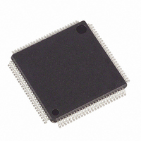
DS21552L+ Maxim Integrated Products, DS21552L+ Datasheet - Page 18

DS21552L+
Manufacturer Part Number
DS21552L+
Description
IC TXRX T1 1-CHIP 5V 100-LQFP
Manufacturer
Maxim Integrated Products
Datasheet
1.DS21352L.pdf
(137 pages)
Specifications of DS21552L+
Function
Single-Chip Transceiver
Interface
E1, HDLC, J1, T1
Number Of Circuits
1
Voltage - Supply
4.75 V ~ 5.25 V
Current - Supply
75mA
Operating Temperature
0°C ~ 70°C
Mounting Type
Surface Mount
Package / Case
100-LQFP
Includes
DSX-1 and CSU Line Build-Out Generator, HDLC Controller, In-Band Loop Code Generator and Detector
Product
Framer
Number Of Transceivers
1
Data Rate
64 Kbps
Supply Voltage (max)
3.465 V
Supply Voltage (min)
3.135 V
Supply Current (max)
75 mA (Typ)
Maximum Operating Temperature
+ 70 C
Minimum Operating Temperature
0 C
Mounting Style
SMD/SMT
Ic Interface Type
Parallel, Serial
Supply Voltage Range
4.75V To 5.25V
Operating Temperature Range
0°C To +70°C
Digital Ic Case Style
LQFP
No. Of Pins
100
Filter Terminals
SMD
Rohs Compliant
Yes
Lead Free Status / RoHS Status
Lead free / RoHS Compliant
Power (watts)
-
Lead Free Status / Rohs Status
Lead free / RoHS Compliant
4.1.2 RECEIVE SIDE PINS
Signal Name:
Signal Description:
Signal Type:
Updated with either FDL data (ESF) or Fs bits (D4) or Z bits (ZBTSI) one RCLK before the start of a frame. See Section 20
for details.
Signal Name:
Signal Description:
Signal Type:
A 4 kHz or 2 kHz (ZBTSI) clock for the RLINK output.
Signal Name:
Signal Description:
Signal Type:
1.544 MHz clock that is used to clock data through the receive side framer.
Signal Name:
Signal Description:
Signal Type:
A 192 kHz clock which pulses high during the LSB of each channel. Synchronous with RCLK when the receive side elastic
store is disabled. Synchronous with RSYSCLK when the receive side elastic store is enabled. Useful for parallel to serial
conversion of channel data.
Signal Name:
Signal Description:
Signal Type:
A user programmable output that can be forced high or low during any of the 24 T1 channels. Synchronous with RCLK when
the receive side elastic store is disabled. Synchronous with RSYSCLK when the receive side elastic store is enabled. Useful for
blocking clocks to a serial UART or LAPD controller in applications where not all T1 channels are used such as Fractional T1,
384K bps service, 768K bps, or ISDN–PRI. Also useful for locating individual channels in drop–and–insert applications, for
external per–channel loopback, and for per–channel conditioning. See Section 13 page 76 for details.
Signal Name:
Signal Description:
Signal Type:
Received NRZ serial data. Updated on rising edges of RCLK when the receive side elastic store is disabled. Updated on the
rising edges of RSYSCLK when the receive side elastic store is enabled.
Signal Name:
Signal Description:
Signal Type:
An extracted pulse, one RCLK wide, is output at this pin which identifies either frame (RCR2.4 = 0) or multiframe (RCR2.4 =
1) boundaries. If set to output frame boundaries then via RCR2.5, RSYNC can also be set to output double–wide pulses on
signaling frames. If the receive side elastic store is enabled via CCR1.2, then this pin can be enabled to be an input via RCR2.3
at which a frame or multiframe boundary pulse is applied. See Section 21 for details.
RLINK
Receive Link Data
Output
RLCLK
Receive Link Clock
Output
RCLK
Receive Clock
Output
RCHCLK
Receive Channel Clock
Output
RCHBLK
Receive Channel Block
Output
RSER
Receive Serial Data
Output
RSYNC
Receive Sync
Input/Output
18 of 137


