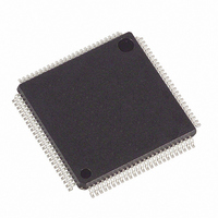
DS21552L+ Maxim Integrated Products, DS21552L+ Datasheet - Page 59

DS21552L+
Manufacturer Part Number
DS21552L+
Description
IC TXRX T1 1-CHIP 5V 100-LQFP
Manufacturer
Maxim Integrated Products
Datasheet
1.DS21352L.pdf
(137 pages)
Specifications of DS21552L+
Function
Single-Chip Transceiver
Interface
E1, HDLC, J1, T1
Number Of Circuits
1
Voltage - Supply
4.75 V ~ 5.25 V
Current - Supply
75mA
Operating Temperature
0°C ~ 70°C
Mounting Type
Surface Mount
Package / Case
100-LQFP
Includes
DSX-1 and CSU Line Build-Out Generator, HDLC Controller, In-Band Loop Code Generator and Detector
Product
Framer
Number Of Transceivers
1
Data Rate
64 Kbps
Supply Voltage (max)
3.465 V
Supply Voltage (min)
3.135 V
Supply Current (max)
75 mA (Typ)
Maximum Operating Temperature
+ 70 C
Minimum Operating Temperature
0 C
Mounting Style
SMD/SMT
Ic Interface Type
Parallel, Serial
Supply Voltage Range
4.75V To 5.25V
Operating Temperature Range
0°C To +70°C
Digital Ic Case Style
LQFP
No. Of Pins
100
Filter Terminals
SMD
Rohs Compliant
Yes
Lead Free Status / RoHS Status
Lead free / RoHS Compliant
Power (watts)
-
Lead Free Status / Rohs Status
Lead free / RoHS Compliant
DS21352/DS21552
multiframe boundary. In this mode, the elastic store must be enabled however the backplane clock can be
either 1.544 MHz or 2.048 MHz.
If the signaling re–insertion mode is enabled, the user can control which channels have signaling re–
insertion performed on a channel–by–channel basis by setting the RPCSI control bit high (CCR4.6) and
then programming the RCHBLK output pin to go high in the channels in which the signaling re–insertion
should not occur. If the RPCSI bit is set low, then signaling re–insertion will occur in all channels when
the signaling re–insertion mode is enabled (RSRE=1). How to control the operation of the RCHBLK
output pin is covered in Section 13.
10.2.1.2 RECEIVE SIGNALING ALL ONES
In both hardware based signaling operating modes, the user has the option to replace all of the extracted
robbed–bit signaling bit positions with ones. This option is enabled via the RFSA1 control bit (CCR4.5)
and it can be invoked on a per–channel basis by setting the RPCSI control bit (CCR4.6) high and then
programming RCHBLK appropriately just like the per–channel signaling re–insertion operates.
10.2.1.3 RECEIVE SIGNALING FREEZE
The signaling data in the four multiframe buffer will be frozen in a known good state upon either a loss of
synchronization (OOF event), carrier loss, or frame slip. This action meets the requirements of BellCore
TR– TSY–000170 for signaling freezing. To allow this freeze action to occur, the RFE control bit
(CCR4.4) should be set high. The user can force a freeze by setting the RFF control bit (CCR4.3) high.
The RSIGF output pin provides a hardware indication that a freeze is in effect. The four multiframe
buffer provides a three multiframe delay in the signaling bits provided at the RSIG pin (and at the RSER
pin if RSRE=1). When freezing is enabled (RFE=1), the signaling data will be held in the last known
good state until the corrupting error condition subsides. When the error condition subsides, the signaling
data will be held in the old state for at least an additional 9 ms (or 4.5 ms in D4 framing mode) before
being allowed to be updated with new signaling data.
10.2.2 TRANSMIT SIDE
Via the THSE control bit (CCR4.2), the framer can be set up to take the signaling data presented at the
TSIG pin and insert the signaling data into the PCM data stream that is being input at the TSER pin. The
user has the ability to control which channels are to have signaling data from the TSIG pin inserted into
them on a channel–by–channel basis by setting the TPCSI control bit (CCR4.1) high. When TPCSI is
enabled, channels in which the TCHBLK output has been programmed to be set high in, will not have
signaling data from the TSIG pin inserted into them. The signaling insertion capabilities of the framer are
available whether the transmit side elastic store is enabled or disabled. If the elastic store is enabled, the
backplane clock (TSYSCLK) can be either 1.544 MHz or 2.048 MHz.
11. PER–CHANNEL CODE (IDLE) GENERATION
Data can be replaced by an idle code on a channel–by–channel basis in the transmit and receive
directions. The transmit direction is from the backplane to the T1 line and is covered in Section11.1. The
receive direction is from the T1 line to the backplane and is covered in Section 11.2.
59 of 137


