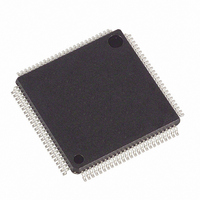
DS21552L+ Maxim Integrated Products, DS21552L+ Datasheet - Page 83

DS21552L+
Manufacturer Part Number
DS21552L+
Description
IC TXRX T1 1-CHIP 5V 100-LQFP
Manufacturer
Maxim Integrated Products
Datasheet
1.DS21352L.pdf
(137 pages)
Specifications of DS21552L+
Function
Single-Chip Transceiver
Interface
E1, HDLC, J1, T1
Number Of Circuits
1
Voltage - Supply
4.75 V ~ 5.25 V
Current - Supply
75mA
Operating Temperature
0°C ~ 70°C
Mounting Type
Surface Mount
Package / Case
100-LQFP
Includes
DSX-1 and CSU Line Build-Out Generator, HDLC Controller, In-Band Loop Code Generator and Detector
Product
Framer
Number Of Transceivers
1
Data Rate
64 Kbps
Supply Voltage (max)
3.465 V
Supply Voltage (min)
3.135 V
Supply Current (max)
75 mA (Typ)
Maximum Operating Temperature
+ 70 C
Minimum Operating Temperature
0 C
Mounting Style
SMD/SMT
Ic Interface Type
Parallel, Serial
Supply Voltage Range
4.75V To 5.25V
Operating Temperature Range
0°C To +70°C
Digital Ic Case Style
LQFP
No. Of Pins
100
Filter Terminals
SMD
Rohs Compliant
Yes
Lead Free Status / RoHS Status
Lead free / RoHS Compliant
Power (watts)
-
Lead Free Status / Rohs Status
Lead free / RoHS Compliant
16. LINE INTERFACE FUNCTION
The line interface function in the DS21352/552 contains three sections; (1) the receiver which handles
clock and data recovery, (2) the transmitter which waveshapes and drives the T1 line, and (3) the jitter
attenuator. Each of the these three sections is controlled by the Line Inter-face Control Register (LICR)
which is described below.
LICR: LINE INTERFACE CONTROL REGISTER (Address=7C Hex)
16.1 RECEIVE CLOCK AND DATA RECOVERY
The DS21352/552 contains a digital clock recovery system. See Figure 3-1 and Figure 16-1 for more
details. The DS21352/552 couples to the receive T1 twisted pair via a 1:1 transformer. See for details.
The 1.544 MHz clock applied to the MCLK pin is internally multiplied by 16 via an internal PLL and fed
to the clock recovery system. The clock recovery system uses the clock from the PLL circuit to form a 16
times oversampler which is used to recover the clock and data. This oversampling technique offers
outstanding jitter tolerance (see Figure 16-4).
Normally, the clock that is output at the RCLKO pin is the recovered clock from the T1 AMI/B8ZS
waveform presented at the RTIP and RRING inputs. When no AMI signal is present at RTIP and RRING,
a Receive Carrier Loss (LRCL) condition will occur and the RCLKO will be sourced from the clock
applied at the MCLK pin. If the jitter attenuator is either placed in the transmit path or is disabled, the
RCLKO output can exhibit slightly shorter high cycles of the clock. This is due to the highly oversampled
digital clock recovery circuitry. If the jitter attenuator is placed in the receive path (as is the case in most
applications), the jitter attenuator restores the RCLK to being close to 50% duty cycle. Please see the
Receive AC Timing Characteristics in section 24 for more details.
SYMBOL
(MSB)
JABDS
L2
EGL
DJA
TPD
JAS
L2
L1
L0
POSITION
L1
LICR.7
LICR.6
LICR.5
LICR.4
LICR.3
LICR.2
LICR.1
LICR.0
NAME AND DESCRIPTION
Line Build Out Select Bit 2. Sets the transmitter build out; see Table 16-1
Line Build Out Select Bit 1. Sets the transmitter build out; see Table 16-1
Line Build Out Select Bit 0. Sets the transmitter build out; see Table 16-1
Receive Equalizer Gain Limit. 0 = –36 dB 1 = –30 dB
Jitter Attenuator Select. 0 = place the jitter attenuator on the receive side 1 = place
the jitter attenuator on the transmit side
Jitter Attenuator Buffer Depth Select 0 = 128 bits 1 = 32 bits (use for delay
sensitive applications)
Disable Jitter Attenuator. 0 = jitter attenuator enabled 1 = jitter attenuator disabled
Transmit Power Down. 0 = normal transmitter operation 1 = powers down the
transmitter and 3-states the TTIP and TRING pins
L0
EGL
83 of 137
JAS
JABDS
DJA
(LSB)
TPD


