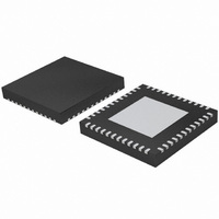
SC16C654BIBS,528 NXP Semiconductors, SC16C654BIBS,528 Datasheet - Page 12

SC16C654BIBS,528
Manufacturer Part Number
SC16C654BIBS,528
Description
IC QUAD UART 64BYTE 48HVQFN
Manufacturer
NXP Semiconductors
Datasheet
1.SC16C654BIBS528.pdf
(58 pages)
Specifications of SC16C654BIBS,528
Features
False-start Bit Detection
Number Of Channels
4, QUART
Fifo's
64 Byte
Voltage - Supply
2.5V, 3.3V, 5V
With Auto Flow Control
Yes
With Irda Encoder/decoder
Yes
With False Start Bit Detection
Yes
With Modem Control
Yes
With Cmos
Yes
Mounting Type
Surface Mount
Package / Case
48-VQFN Exposed Pad, 48-HVQFN, 48-SQFN, 48-DHVQFN
Lead Free Status / RoHS Status
Lead free / RoHS Compliant
Other names
935279073528
SC16C654BIBS-F
SC16C654BIBS-F
SC16C654BIBS-F
SC16C654BIBS-F
Philips Semiconductors
Table 2:
9397 750 14965
Product data sheet
Symbol
INTSEL
IOR
IOW
IRQ
n.c.
RESET,
RESET
Pin
PLCC68 LQFP64 HVQFN48 LFBGA6
65
52
18
15
21, 49,
52, 54,
55, 65
37
Pin description
-
40
9
-
-
27
…continued
-
33
7
4
-
20
4
-
F9
F1
-
-
J7
5 V, 3.3 V and 2.5 V quad UART, 5 Mbit/s (max.) with 64-byte FIFOs
Rev. 02 — 20 June 2005
Type Description
I
I
I
O
-
I
Interrupt Select (active HIGH, with internal pull-down).
This function is associated with the 16 mode only. When the
16 mode is selected, this pin can be used in conjunction with
MCR[3] to enable or disable the 3-state interrupts,
INTA to INTD, or override MCR[3] and force continuous
interrupts. Interrupt outputs are enabled continuously by
making this pin a logic 1. Making this pin a logic 0 allows
MCR[3] to control the 3-state interrupt output. In this mode,
MCR[3] is set to a logic 1 to enable the 3-state outputs. This
pin is disabled in the 68 mode. Due to pin limitations on the
64-pin packages, this pin is not available. To cover this
limitation, the SC16C654DBIB64 version operates in the
continuous interrupt enable mode by bonding this pin to V
internally. The SC16C654BIB64 operates with MCR[3]
control by bonding this pin to GND.
Input/Output Read strobe (active LOW). This function is
associated with the 16 mode only. A logic 0 transition on this
pin will load the contents of an internal register defined by
address bits A[0:2] onto the SC16C654B/654DB data bus
(D[0:7]) for access by external CPU. This pin is disabled in
the 68 mode.
Input/Output Write strobe (active LOW). This function is
associated with the 16 mode only. A logic 0 transition on this
pin will transfer the contents of the data bus (D[0:7]) from the
external CPU to an internal register that is defined by
address bits A[0:2]. When the 68 mode is selected
(PLCC68), this pin functions as R/W (see definition under
R/W).
Interrupt Request or Interrupt ‘A’. This function is
associated with the 68 mode only. In the 68 mode, interrupts
from UART channels A-D are wire-ORed internally to
function as a single IRQ interrupt. This pin transitions to a
logic 0 (if enabled by the interrupt enable register) whenever
a UART channel(s) requires service. Individual channel
interrupt status can be determined by addressing each
channel through its associated internal register, using CS
and A[3:4]. In the 68 mode, and external pull-up resistor
must be connected between this pin and V
of this pin changes to INTA when operating in the 16 mode
(see definition under INTA).
not connected
Reset. In the 16 mode, a logic 1 on this pin will reset the
internal registers and all the outputs. The UART transmitter
output and the receiver input will be disabled during reset
time. (See
conditions”
(68 mode), this pin functions similarly, but as an inverted
reset interface signal, RESET.
Section 7.11 “SC16C654B/654DB external reset
for initialization details.) When 16/68 is a logic 0
SC16C654B/654DB
© Koninklijke Philips Electronics N.V. 2005. All rights reserved.
CC
. The function
12 of 58
CC


