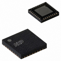
SC16C550BIBS,157 NXP Semiconductors, SC16C550BIBS,157 Datasheet - Page 10

SC16C550BIBS,157
Manufacturer Part Number
SC16C550BIBS,157
Description
IC UART SOT617-1
Manufacturer
NXP Semiconductors
Datasheet
1.SC16C550BIA44518.pdf
(48 pages)
Specifications of SC16C550BIBS,157
Features
Programmable
Number Of Channels
1, UART
Fifo's
16 Byte
Voltage - Supply
2.5V, 3.3V, 5V
With Auto Flow Control
Yes
With False Start Bit Detection
Yes
With Modem Control
Yes
With Cmos
Yes
Mounting Type
Surface Mount
Package / Case
32-VFQFN Exposed Pad
Lead Free Status / RoHS Status
Lead free / RoHS Compliant
Other names
935279497157
SC16C550BIBS
SC16C550BIBS
SC16C550BIBS
SC16C550BIBS
NXP Semiconductors
SC16C550B_5
Product data sheet
6.1 Internal registers
6.2 FIFO operation
The SC16C550B provides 12 internal registers for monitoring and control. These registers
are shown in
interrupt status and control registers (IER/ISR), a FIFO Control Register (FCR), line status
and control registers (LCR/LSR), modem status and control registers (MCR/MSR),
programmable data rate (clock) control registers (DLL/DLM), and a user accessible
scratchpad register (SPR). Register functions are more fully described in the following
paragraphs.
Table 3.
[1]
[2]
The 16-byte transmit and receive data FIFOs are enabled by the FIFO Control Register
bit 0 (FCR[0]). With 16C550 devices, the user can set the receive trigger level, but not the
transmit trigger level. The receiver FIFO section includes a time-out function to ensure
data is delivered to the external CPU. An interrupt is generated whenever the Receive
Holding Register (RHR) has not been read following the loading of a character or the
receive trigger level has not been reached.
Table 4.
A2
General register set (THR/RHR, IER/ISR, MCR/MSR, FCR/LSR, SPR)
0
0
0
0
1
1
1
1
Baud rate register set (DLL/DLM)
0
0
Selected trigger level
(characters)
1
4
8
14
These registers are accessible only when LCR[7] is a logic 0.
These registers are accessible only when LCR[7] is a logic 1.
A1
0
0
1
1
0
0
1
1
0
0
Internal registers decoding
Flow control mechanism
Table
A0
0
1
0
1
0
1
0
1
0
1
3. These registers function as data holding registers (THR/RHR),
Rev. 05 — 1 October 2008
Read mode
Receive Holding Register
Interrupt Enable Register
Interrupt Status Register
Line Control Register
Modem Control Register
Line Status Register
Modem Status Register
Scratchpad Register
LSB of Divisor Latch
MSB of Divisor Latch
INT pin activation
1
4
8
14
[2]
5 V, 3.3 V and 2.5 V UART with 16-byte FIFOs
Negate RTS
1
4
8
14
Write mode
Transmit Holding Register
Interrupt Enable Register
FIFO Control Register
Line Control Register
Modem Control Register
n/a
n/a
Scratchpad Register
LSB of Divisor Latch
MSB of Divisor Latch
SC16C550B
[1]
© NXP B.V. 2008. All rights reserved.
Assert RTS
0
0
0
0
10 of 48


