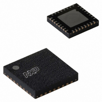
SC16C550BIBS,157 NXP Semiconductors, SC16C550BIBS,157 Datasheet - Page 21

SC16C550BIBS,157
Manufacturer Part Number
SC16C550BIBS,157
Description
IC UART SOT617-1
Manufacturer
NXP Semiconductors
Datasheet
1.SC16C550BIA44518.pdf
(48 pages)
Specifications of SC16C550BIBS,157
Features
Programmable
Number Of Channels
1, UART
Fifo's
16 Byte
Voltage - Supply
2.5V, 3.3V, 5V
With Auto Flow Control
Yes
With False Start Bit Detection
Yes
With Modem Control
Yes
With Cmos
Yes
Mounting Type
Surface Mount
Package / Case
32-VFQFN Exposed Pad
Lead Free Status / RoHS Status
Lead free / RoHS Compliant
Other names
935279497157
SC16C550BIBS
SC16C550BIBS
SC16C550BIBS
SC16C550BIBS
NXP Semiconductors
SC16C550B_5
Product data sheet
7.3.2 FIFO mode
Table 11.
Bit
7:6
5:4
3
2
1
0
Symbol
FCR[7] (MSB),
FCR[6] (LSB)
FCR[5] (MSB),
FCR[4] (LSB)
FCR[3]
FCR[2]
FCR[1]
FCR[0]
FIFO Control Register bits description
Rev. 05 — 1 October 2008
Description
RX trigger. These bits are used to set the trigger level for the receive
FIFO interrupt.
An interrupt is generated when the number of characters in the FIFO
equals the programmed trigger level. However, the FIFO will continue to
be loaded until it is full. Refer to
not used; set to 00
DMA mode select.
Transmit operation in mode ‘0’: When the SC16C550B is in the
16C450 mode (FIFOs disabled; FCR[0] = logic 0) or in the FIFO mode
(FIFOs enabled; FCR[0] = logic 1; FCR[3] = logic 0), and when there are
no characters in the transmit FIFO or transmit holding register, the
TXRDY pin will be a logic 0. Once active, the TXRDY pin will go to a
logic 1 after the first character is loaded into the transmit holding register.
Receive operation in mode ‘0’: When the SC16C550B is in 16C450
mode, or in the FIFO mode (FCR[0] = logic 1; FCR[3] = logic 0) and there
is at least one character in the receive FIFO, the RXRDY pin will be a
logic 0. Once active, the RXRDY pin will go to a logic 1 when there are no
more characters in the receiver.
Transmit operation in mode ‘1’: When the SC16C550B is in FIFO
mode (FCR[0] = logic 1; FCR[3] = logic 1), the TXRDY pin will be a
logic 1 when the transmit FIFO is completely full. It will be a logic 0 if the
transmit FIFO is completely empty.
Receive operation in mode ‘1’: When the SC16C550B is in FIFO mode
(FCR[0] = logic 1; FCR[3] = logic 1) and the trigger level has been
reached, or a Receive Time-Out has occurred, the RXRDY pin will go to
a logic 0. Once activated, it will go to a logic 1 after there are no more
characters in the FIFO.
TX FIFO reset.
RX FIFO reset.
FIFO enable.
logic 0 = set DMA mode ‘0’ (normal default condition)
logic 1 = set DMA mode ‘1’
logic 0 = no FIFO transmit reset (normal default condition)
logic 1 = clears the contents of the transmit FIFO and resets the FIFO
counter logic (the transmit shift register is not cleared or altered). This
bit will return to a logic 0 after clearing the FIFO.
logic 0 = no FIFO receive reset (normal default condition)
logic 1 = clears the contents of the receive FIFO and resets the FIFO
counter logic (the receive shift register is not cleared or altered). This
bit will return to a logic 0 after clearing the FIFO.
logic 0 = disable the transmit and receive FIFO (normal default
condition)
logic 1 = enable the transmit and receive FIFO. This bit must be a ‘1’
when other FCR bits are written to, or they will not be
programmed.
5 V, 3.3 V and 2.5 V UART with 16-byte FIFOs
Table
12.
SC16C550B
© NXP B.V. 2008. All rights reserved.
21 of 48


