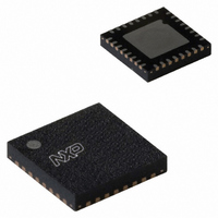
SC16C550BIBS,157 NXP Semiconductors, SC16C550BIBS,157 Datasheet - Page 19

SC16C550BIBS,157
Manufacturer Part Number
SC16C550BIBS,157
Description
IC UART SOT617-1
Manufacturer
NXP Semiconductors
Datasheet
1.SC16C550BIA44518.pdf
(48 pages)
Specifications of SC16C550BIBS,157
Features
Programmable
Number Of Channels
1, UART
Fifo's
16 Byte
Voltage - Supply
2.5V, 3.3V, 5V
With Auto Flow Control
Yes
With False Start Bit Detection
Yes
With Modem Control
Yes
With Cmos
Yes
Mounting Type
Surface Mount
Package / Case
32-VFQFN Exposed Pad
Lead Free Status / RoHS Status
Lead free / RoHS Compliant
Other names
935279497157
SC16C550BIBS
SC16C550BIBS
SC16C550BIBS
SC16C550BIBS
NXP Semiconductors
SC16C550B_5
Product data sheet
7.1 Transmit Holding Register (THR) and Receive Holding Register (RHR)
7.2 Interrupt Enable Register (IER)
The serial transmitter section consists of an 8-bit Transmit Holding Register (THR) and
Transmit Shift Register (TSR). The status of the THR is provided in the Line Status
Register (LSR). Writing to the THR transfers the contents of the data bus (D[7:0]) to the
THR, providing that the THR or TSR is empty. The THR empty flag in the LSR register will
be set to a logic 1 when the transmitter is empty or when data is transferred to the TSR.
Note that a write operation can be performed when the THR empty flag is set
(logic 0 = FIFO full; logic 1 = at least one FIFO location available).
The serial receive section also contains an 8-bit Receive Holding Register (RHR).
Receive data is removed from the SC16C550B and receive FIFO by reading the RHR
register. The receive section provides a mechanism to prevent false starts. On the falling
edge of a start or false start bit, an internal receiver counter starts counting clocks at the
16 clock rate. After 7
start bit. At this time the start bit is sampled, and if it is still a logic 0 it is validated.
Evaluating the start bit in this manner prevents the receiver from assembling a false
character. Receiver status codes will be posted in the LSR.
The Interrupt Enable Register (IER) masks the interrupts from receiver ready, transmitter
empty, line status and modem status registers. These interrupts would normally be seen
on the INT output pin.
Table 10.
Bit
7:4
3
2
1
0
Symbol
IER[7:4]
IER[3]
IER[2]
IER[1]
IER[0]
Interrupt Enable Register bits description
Description
not used
Modem Status Interrupt.
Receive Line Status interrupt. This interrupt will be issued whenever a fully
assembled receive character is transferred from RSR to the RHR/FIFO, that is,
data ready, LSR[0].
Transmit Holding Register interrupt. This interrupt will be issued whenever the
THR is empty, and is associated with LSR[1].
Receive Holding Register interrupt. This interrupt will be issued when the FIFO
has reached the programmed trigger level, or is cleared when the FIFO drops
below the trigger level in the FIFO mode of operation.
logic 0 = disable the modem status register interrupt (normal default
condition)
logic 1 = enable the modem status register interrupt
logic 0 = disable the receiver line status interrupt (normal default condition)
logic 1 = enable the receiver line status interrupt
logic 0 = disable the transmitter empty interrupt (normal default condition)
logic 1 = enable the transmitter empty interrupt
logic 0 = disable the receiver ready interrupt (normal default condition)
logic 1 = enable the receiver ready interrupt
1
Rev. 05 — 1 October 2008
2
clocks, the start bit time should be shifted to the center of the
5 V, 3.3 V and 2.5 V UART with 16-byte FIFOs
SC16C550B
© NXP B.V. 2008. All rights reserved.
19 of 48


