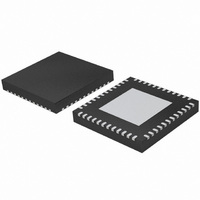
SC16C554BIBS,557 NXP Semiconductors, SC16C554BIBS,557 Datasheet - Page 13

SC16C554BIBS,557
Manufacturer Part Number
SC16C554BIBS,557
Description
IC UART QUAD SOT778-3
Manufacturer
NXP Semiconductors
Datasheet
1.SC16C554BIB80528.pdf
(58 pages)
Specifications of SC16C554BIBS,557
Number Of Channels
4, QUART
Fifo's
16 Byte
Voltage - Supply
2.5V, 3.3V, 5V
With Auto Flow Control
Yes
With False Start Bit Detection
Yes
With Modem Control
Yes
With Cmos
Yes
Mounting Type
Surface Mount
Package / Case
48-VQFN Exposed Pad, 48-HVQFN, 48-SQFN, 48-DHVQFN
Lead Free Status / RoHS Status
Lead free / RoHS Compliant
Other names
935279072557
SC16C554BIBS
SC16C554BIBS
SC16C554BIBS
SC16C554BIBS
NXP Semiconductors
Table 2.
SC16C554B_554DB
Product data sheet
Symbol
RESET
(RESET)
RIA
RIB
RIC
RID
RTSA
RTSB
RTSC
RTSD
R/W
RXA
RXB
RXC
RXD
RXRDY
Pin description
Pin
PLCC68 LQFP64 LQFP80 HVQFN48
37
8
28
42
62
14
22
48
56
18
7
29
41
63
38
27
63
19
30
50
5
13
36
44
-
62
20
29
51
-
…continued
53
18
43
58
3
26
35
66
75
-
17
44
57
4
54
All information provided in this document is subject to legal disclaimers.
5 V, 3.3 V and 2.5 V quad UART, 5 Mbit/s (max.) with 16-byte FIFOs
20
-
-
23
-
3
11
29
-
7
48
13
22
38
-
Rev. 4 — 8 June 2010
Type
I
I
I
I
I
O
O
O
O
I
I
I
I
I
O
Description
Reset. In the 16 mode, a logic 1 on this pin will reset
the internal registers and all the outputs. The UART
transmitter output and the receiver input will be
disabled during reset time. (See
“SC16C554B/554DB external reset conditions”
initialization details.) When 16/68 is a logic 0
(68 mode), this pin functions similarly, bus as an
inverted reset interface signal, RESET.
Ring Indicator (active LOW). These inputs are
associated with individual UART channels, A to D. A
logic 0 on this pin indicates the modem has received a
ringing signal from the telephone line. A logic 1
transition on this input pin will generate an interrupt.
Request to Send (active LOW). These outputs are
associated with individual UART channels, A to D. A
logic 0 on the RTSn pin indicates the transmitter has
data ready and waiting to send. Writing a logic 1 in the
Modem Control Register MCR[1] will set this pin to a
logic 0, indicating data is available. After a reset this pin
will be set to a logic 1. This pin only affects the transmit
and receive operations when auto-RTS function is
enabled via MCR[5] for hardware flow control
operation.
Read/Write strobe. This function is associated with the
68 mode only. This pin provides the combined functions
for Read or Write strobes.
Logic 1 = Read from UART register selected by CS and
A0 to A4.
Logic 0 = Write to UART register selected by CS and
A0 to A4.
Receive data input RXA to RXD. These inputs are
associated with individual serial channel data to the
SC16C554B/554DB. The RXn signal will be a logic 1
during reset, idle (no data), or when the transmitter is
disabled. During the local Loopback mode, the RXn
input pin is disabled and TX data is connected to the
UART RX input internally.
Receive Ready (active LOW). RXRDY contains the
wire-ORed status of all four receive channel FIFOs,
RXRDYA to RXRDYD. A logic 0 indicates receive data
ready status, that is, the RHR is full, or the FIFO has
one or more RX characters available for unloading.
This pin goes to a logic 1 when the FIFO/RHR is empty,
or when there are no more characters available in
either the FIFO or RHR. Individual channel RX status is
read by examining individual internal registers via CS
and A0 to A4 pin functions. The RXRDY pin is not
available on the HVQFN48 package.
SC16C554B/554DB
Section 7.10
© NXP B.V. 2010. All rights reserved.
for
13 of 58


