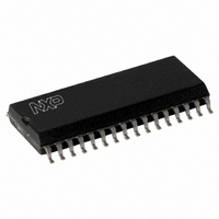
TFA9810T/N1,118 NXP Semiconductors, TFA9810T/N1,118 Datasheet - Page 15

TFA9810T/N1,118
Manufacturer Part Number
TFA9810T/N1,118
Description
IC AMP AUDIO 15W STER D 32SOIC
Manufacturer
NXP Semiconductors
Type
Class Dr
Datasheet
1.TFA9810TN1118.pdf
(29 pages)
Specifications of TFA9810T/N1,118
Output Type
2-Channel (Stereo)
Package / Case
32-SOIC (7.5mm Width)
Max Output Power X Channels @ Load
15W x 2 @ 8 Ohm
Voltage - Supply
8 V ~ 20 V
Features
Short-Circuit and Thermal Protection
Mounting Type
Surface Mount
Product
Class-D
Output Power
15 W
Available Set Gain
19.7 dB
Thd Plus Noise
0.04 %
Operating Supply Voltage
12 V
Maximum Power Dissipation
2500 mW
Maximum Operating Temperature
+ 85 C
Mounting Style
SMD/SMT
Audio Load Resistance
8 Ohms
Input Bias Current (max)
1 uA
Input Signal Type
Differential
Minimum Operating Temperature
- 40 C
Output Signal Type
Differential
Supply Type
Single
Supply Voltage (max)
20 V
Supply Voltage (min)
8 V
Lead Free Status / RoHS Status
Lead free / RoHS Compliant
Other names
935280404118
TFA9810T-T
TFA9810T-T
TFA9810T-T
TFA9810T-T
NXP Semiconductors
11. Thermal characteristics
Table 8.
[1]
[2]
12. Characteristics
Table 9.
T
TFA9810_3
Product data sheet
Symbol
R
Symbol
Supply voltage
V
I
I
ENABLE input
V
V
off
q
amb
P
IL
IH
th(j-a)
j-lead
j-top
Measured in a JEDEC high K-factor test board (standard EIA/JESD 51-7) in free air with natural convection.
Strongly depends on where the measurement is taken on the case.
= 25 C; V
Characteristics
Static characteristics
Parameter
supply voltage
off-state current
quiescent current
LOW-level input voltage
HIGH-level input voltage with respect to V
Parameter
thermal resistance
from junction to
ambient
thermal
characterization
parameter from
junction to lead
thermal
characterization
parameter from
junction to top of
package
P
12.1 Static characteristics
= 12 V; f
Table 7.
In accordance with the Absolute Maximum Rating System (IEC 60134).
Symbol Parameter
V
V
osc
x
esd
= 550 kHz;
voltage on pin x
electrostatic discharge voltage
Limiting values
Conditions
SO32. JEDEC test board
SO32. Two-layer application
board
SO32
SO32
Conditions
V
off mode
with load, filter, and snubbers
connected
with respect to V
Figure 33
P
= V
DDPx
Rev. 03 — 20 February 2008
unless otherwise specified
V
…continued
SSPx
SSD
SSD
[1] [2]
Conditions
DIAG
IN1P - IN1N
IN2P - IN2N
all other pins
VINX with
respect to
other pins
all other pins
[1]
[1]
Min
8
-
-
3
Min
-
-
0.3
Min
V
V
12
12
1500
2000
Typ
41
44
4
Typ
12
110
35
-
-
SS
SS
Audio amplifier 2 x 12 W
0.3
0.3
Max
+12
+12
+12
V
+1500
+2000
Max
44
-
30
8
Max
20
200
45
+0.8
V
© NXP B.V. 2008. All rights reserved.
TFA9810
DD
P
+ 0.3
Unit
K/W
K/W
K/W
K/W
Unit
V
mA
V
V
Unit
V
V
V
V
V
V
15 of 29
A


