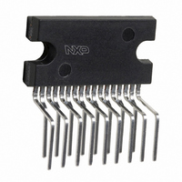
TDA8946AJ/N2,112 NXP Semiconductors, TDA8946AJ/N2,112 Datasheet - Page 8

TDA8946AJ/N2,112
Manufacturer Part Number
TDA8946AJ/N2,112
Description
IC AMP AUDIO PWR 15W STER 17SIL
Manufacturer
NXP Semiconductors
Type
Class ABr
Datasheet
1.TDA8946AJN2112.pdf
(20 pages)
Specifications of TDA8946AJ/N2,112
Output Type
2-Channel (Stereo)
Package / Case
17-SIL (Bent and Staggered Leads)
Max Output Power X Channels @ Load
15W x 2 @ 8 Ohm
Voltage - Supply
4.5 V ~ 18 V
Features
Depop, Mute, Short-Circuit and Thermal Protection, Standby
Mounting Type
Through Hole
Product
Class-AB
Output Power
15 W
Available Set Gain
30 dB
Thd Plus Noise
0.07 %
Operating Supply Voltage
18 V
Maximum Power Dissipation
28000 mW
Maximum Operating Temperature
+ 85 C
Mounting Style
SMD/SMT
Audio Load Resistance
8 Ohms
Input Signal Type
Differential
Minimum Operating Temperature
- 40 C
Output Signal Type
Differential
Supply Type
Single
Supply Voltage (max)
18 V
Supply Voltage (min)
4.5 V
Lead Free Status / RoHS Status
Lead free / RoHS Compliant
Other names
568-3456-5
935270283112
TDA8946AJU
935270283112
TDA8946AJU
Philips Semiconductors
11. Static characteristics
Table 7:
V
[1]
[2]
[3]
9397 750 09434
Product data
Symbol
V
I
I
V
V
I
V
I
q
stb
MODE
GC
CC
Fig 4. Quiescent current as function of supply
CC
O
V
MODE
GC
handbook, halfpage
OUT
= 18 V; T
With a load connected at the outputs the quiescent current will increase, the maximum of this increase being equal to the differential
output voltage offset
The DC output voltage with respect to ground is approximately 0.5V
V
(mA)
[3]
I q
OUT
50
40
30
20
10
voltage.
0
= V
0
Static characteristics
amb
OUT+
= 25 C; R
Parameter
supply voltage
quiescent supply current
standby supply current
DC output voltage
differential output voltage
offset
mode selection input voltage operating mode
mode selection input current 0 < V
gain control voltage (pin GC) pin GC not connected
current into pin GC
4
V
OUT
V
OUT
8
L
.
= 8 ; V
) divided by the load resistance (R
12
MODE
16
= 0 V; V
V CC (V)
MGW611
Conditions
operating
R
V
mute mode
standby mode
V
20
L
MODE
GC
Rev. 01 — 01 March 2002
i
=
= 0 V; measured in test circuit
= 0 V
MODE
= V
CC
< V
L
).
CC
Fig 5. Quiescent current as function of mode voltage.
CC
handbook, halfpage
2 x 15 W BTL audio amplifier with DC gain control
.
(mA)
V
I q
CC
50
40
30
20
10
0
= 18 V
0
[1]
[2]
Min
4.5
-
-
-
-
0
3.5
V
-
-
-
CC
4
Figure
0.5
8
© Koninklijke Philips Electronics N.V. 2002. All rights reserved.
15; unless otherwise specified.
Typ
18
45
-
9
-
-
-
-
-
2.75
600
12
TDA8946AJ
16
V MODE (V)
Max
18
55
-
170
V
V
-
10
1.0
20
-
CC
CC
MGW612
1.5
20
8 of 20
Unit
V
mA
V
mV
V
V
V
V
A
A
A


