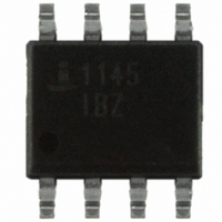
HFA1145IBZ Intersil, HFA1145IBZ Datasheet - Page 5

HFA1145IBZ
Manufacturer Part Number
HFA1145IBZ
Description
IC OPAMP CFA 330MHZ LP 8-SOIC
Manufacturer
Intersil
Datasheet
1.HFA1145IBZ.pdf
(13 pages)
Specifications of HFA1145IBZ
Applications
Current Feedback
Number Of Circuits
1
-3db Bandwidth
330MHz
Slew Rate
2100 V/µs
Current - Supply
5.8mA
Current - Output / Channel
60mA
Voltage - Supply, Single/dual (±)
9 V ~ 11 V, ±4.5 V ~ 5.5 V
Mounting Type
Surface Mount
Package / Case
8-SOIC (0.154", 3.90mm Width)
Rohs Compliant
Yes
Lead Free Status / RoHS Status
Lead free / RoHS Compliant
Available stocks
Company
Part Number
Manufacturer
Quantity
Price
Company:
Part Number:
HFA1145IBZ
Manufacturer:
Intersil
Quantity:
882
Part Number:
HFA1145IBZ
Manufacturer:
INTERSIL
Quantity:
20 000
Electrical Specifications
NOTES:
Application Information
Optimum Feedback Resistor
Although a current feedback amplifier’s bandwidth
dependency on closed loop gain isn’t as severe as that of a
voltage feedback amplifier, there can be an appreciable
decrease in bandwidth at higher gains. This decrease may be
minimized by taking advantage of the current feedback
amplifier’s unique relationship between bandwidth and R
current feedback amplifiers require a feedback resistor, even
for unity gain applications, and R
internal compensation capacitor, sets the dominant pole of the
frequency response. Thus, the amplifier’s bandwidth is
inversely proportional to R
for R
stability, resulting in excessive peaking and overshoot (Note:
Capacitive feedback will cause the same problems due to the
feedback impedance decrease at higher frequencies). At
higher gains, however, the amplifier is more stable so R
be decreased in a trade-off of stability for bandwidth.
The table below lists recommended R
gains, and the expected bandwidth. For a gain of +1, a
resistor (
peaking and increase stability.
DISABLE Input Logic High Current
Output Disable Time (Note 6)
Output Enable Time (Note 6)
Disabled Output Capacitance
Disabled Output Leakage
Off Isolation
(V
POWER SUPPLY CHARACTERISTICS
Power Supply Range
Power Supply Current (Note 6)
3. Test Level: A. Production Tested; B. Typical or Guaranteed Limit Based on Characterization; C. Design Typical for Information Only.
4. Undershoot dominates for output signal swings below GND (e.g. 0.5V
5. Slew rates are asymmetrical if the output swings below GND (e.g. a bipolar signal). Positive unipolar output signals have symmetric positive and
6. See Typical Performance Curves for more information.
DISABLE
condition. See the “Application Information” section for details.
negative slew rates comparable to the +SR specification. See the “Application Information” section, and the pulse response graphs for details.
F
= 510Ω at a gain of +2. Decreasing R
+
R
= 0V, V
S
) in series with +IN is required to reduce gain
PARAMETER
IN
= 1V
P-P
F
. The HFA1145 design is optimized
, Note 6)
5
F
V
, in conjunction with the
SUPPLY
F
values for various
= ±5V, A
F
V
V
V
V
V
V
V
V
At 5MHz
At 25MHz
decreases
DISABLE
IN
DISABLE
IN
DISABLE
DISABLE
DISABLE
OUT
= ±1V,
= ±1V,
V
TEST CONDITIONS
= ±3V
= +1, R
= 5V
= 2.4V to 0V
= 0V to 2.4V
= 0V
= 0V, V
F
F
. All
can
F
HFA1145
= 510Ω, R
IN
=
±
P-P
2V,
L
), yielding a higher overshoot limit compared to the V
Non-inverting Input Source Impedance
For best operation, the DC source impedance seen by the
non-inverting input should be ≥50Ω. This is especially
important in inverting gain configurations where the non-
inverting input would normally be connected directly to GND.
DISABLE Input TTL Compatibility
The HFA1145 derives an internal GND reference for the
digital circuitry as long as the power supplies are
symmetrical about GND. With symmetrical supplies the
digital switching threshold (V
0.8)/2) is 1.4V, which ensures the TTL compatibility of the
DISABLE input. If asymmetrical supplies (e.g. +10V, 0V) are
utilized, the switching threshold becomes:
and the V
= 100Ω, Unless Otherwise Specified (Continued)
V
TH
(A
GAIN
+10
(NOTE 3)
+1
+2
+5
-1
=
CL
LEVEL
TEST
V+
-------------------
)
C
A
B
B
B
A
B
B
A
A
IH
2
+
V-
and V
+
TEMP. (°C)
510 (+R S = 510Ω)
1.4V
IL
Full
Full
Full
25
25
25
25
25
25
25
levels will be V
R
425
510
200
180
F
(Ω)
±4.5
MIN
TH
-
-
-
-
-
-
-
-
-
= (V
TH
TYP
IH
180
2.5
-75
-60
5.8
5.9
35
1
3
-
± 0.6V, respectively.
+ V
BANDWIDTH
IL
MAX
)/2 = (2.0 +
±5.5
6.1
6.3
15
10
(MHz)
-
-
-
-
-
OUT
300
270
330
300
130
= 0 to 0.5V
June 1, 2006
UNITS
FN3955.5
mA
mA
μA
μA
dB
dB
ns
pF
ns
V


