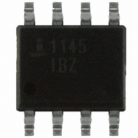
HFA1145IBZ Intersil, HFA1145IBZ Datasheet - Page 6

HFA1145IBZ
Manufacturer Part Number
HFA1145IBZ
Description
IC OPAMP CFA 330MHZ LP 8-SOIC
Manufacturer
Intersil
Datasheet
1.HFA1145IBZ.pdf
(13 pages)
Specifications of HFA1145IBZ
Applications
Current Feedback
Number Of Circuits
1
-3db Bandwidth
330MHz
Slew Rate
2100 V/µs
Current - Supply
5.8mA
Current - Output / Channel
60mA
Voltage - Supply, Single/dual (±)
9 V ~ 11 V, ±4.5 V ~ 5.5 V
Mounting Type
Surface Mount
Package / Case
8-SOIC (0.154", 3.90mm Width)
Rohs Compliant
Yes
Lead Free Status / RoHS Status
Lead free / RoHS Compliant
Available stocks
Company
Part Number
Manufacturer
Quantity
Price
Company:
Part Number:
HFA1145IBZ
Manufacturer:
Intersil
Quantity:
882
Part Number:
HFA1145IBZ
Manufacturer:
INTERSIL
Quantity:
20 000
Optional GND Pad (Die Use Only) for
TTL Compatibility
The die version of the HFA1145 provides the user with a GND
pad for setting the disable circuitry GND reference. With
symmetrical supplies the GND pad may be left unconnected, or
tied directly to GND. If asymmetrical supplies (e.g. +10V, 0V)
are utilized, and TTL compatibility is desired, die users must
connect the GND pad to GND. With an external GND, the
DISABLE input is TTL compatible regardless of supply voltage
utilized.
Pulse Undershoot and Asymmetrical Slew Rates
The HFA1145 utilizes a quasi-complementary output stage to
achieve high output current while minimizing quiescent supply
current. In this approach, a composite device replaces the
traditional PNP pulldown transistor. The composite device
switches modes after crossing 0V, resulting in added distortion
for signals swinging below ground, and an increased
undershoot on the negative portion of the output waveform
(See Figures 5, 8, and 11). This undershoot isn’t present for
small bipolar signals, or large positive signals. Another artifact
of the composite device is asymmetrical slew rates for output
signals with a negative voltage component. The slew rate
degrades as the output signal crosses through 0V (See Figures
5, 8, and 11), resulting in a slower overall negative slew rate.
Positive only signals have symmetrical slew rates as illustrated
in the large signal positive pulse response graphs (See Figures
4, 7, and 10).
PC Board Layout
This amplifier’s frequency response depends greatly on the
care taken in designing the PC board. The use of low
inductance components such as chip resistors and chip
capacitors is strongly recommended, while a solid
ground plane is a must!
Attention should be given to decoupling the power supplies.
A large value (10μF) tantalum in parallel with a small value
(0.1μF) chip capacitor works well in most cases.
Terminated microstrip signal lines are recommended at the
device’s input and output connections. Capacitance,
parasitic or planned, connected to the output must be
minimized, or isolated as discussed in the next section.
Care must also be taken to minimize the capacitance to
ground at the amplifier’s inverting input (-IN), as this
capacitance causes gain peaking, pulse overshoot, and if
large enough, instability. To reduce this capacitance, the
designer should remove the ground plane under traces
connected to -IN, and keep connections to -IN as short as
possible.
An example of a good high frequency layout is the Evaluation
Board shown in Figure 2.
6
HFA1145
Driving Capacitive Loads
Capacitive loads, such as an A/D input, or an improperly
terminated transmission line will degrade the amplifier’s
phase margin resulting in frequency response peaking and
possible oscillations. In most cases, the oscillation can be
avoided by placing a resistor (R
prior to the capacitance.
Figure 1 details starting points for the selection of this
resistor. The points on the curve indicate the R
combinations for the optimum bandwidth, stability, and
settling time, but experimental fine tuning is recommended.
Picking a point above or to the right of the curve yields an
overdamped response, while points below or left of the curve
indicate areas of underdamped performance.
R
system bandwidth well below the amplifier bandwidth of
270MHz (for A
illustrated in the curves), the maximum bandwidth is obtained
without sacrificing stability. In spite of this, the bandwidth
decreases as the load capacitance increases. For example, at
A
limited to 180MHz, and bandwidth drops to 75MHz at A
R
Evaluation Board
The performance of the HFA1145 may be evaluated using
the HFA11XX Evaluation Board and a SOIC to DIP adaptor
like the Aries Electronics Part Number 14-350000-10. The
layout and schematic of the board are shown in Figure 2.
The V
pin, but note that this connection has no 50
order evaluation boards (part number HFA11XXEVAL),
please contact your local sales office.
V
S
S
FIGURE 1. RECOMMENDED SERIES OUTPUT RESISTOR vs
= +1, R
50
40
30
20
10
and C
= 8Ω, C
0
0
H
connection may be used to exercise the DISABLE
L
S
form a low pass network at the output, thus limiting
L
50
LOAD CAPACITANCE
= 62Ω, C
= 400pF.
V
= +1). By decreasing R
100
A
LOAD CAPACITANCE (pF)
L
V
= 40pF, the overall bandwidth is
= +2
150
A
V
200
= +1
S
) in series with the output
250
S
as C
Ω
300
L
termination. To
S
increases (as
and C
350
June 1, 2006
V
FN3955.5
L
= +1,
400


