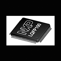
LPC2157_2158 NXP Semiconductors, LPC2157_2158 Datasheet - Page 24

LPC2157_2158
Manufacturer Part Number
LPC2157_2158
Description
The LPC2157/2158 is a multi-chip module consisting of a LPC2138/2148 single-chipmicrocontroller combined with a PCF8576D Universal LCD driver in a low-cost 100-pinpackage
Manufacturer
NXP Semiconductors
Datasheet
1.LPC2157_2158.pdf
(45 pages)
NXP Semiconductors
LPC2157_2158_2
Product data sheet
6.19.1 Crystal oscillator
6.19.2 PLL
6.19.3 Reset and wake-up timer
6.19 System control
On-chip integrated oscillator operates with external crystal in range of 1 MHz to 25 MHz.
The oscillator output frequency is called f
referred to as CCLK for purposes of rate equations, etc. f
unless the PLL is running and connected. Refer to
information.
The PLL accepts an input clock frequency in the range of 10 MHz to 25 MHz. The input
frequency is multiplied up into the range of 10 MHz to 60 MHz with a Current Controlled
Oscillator (CCO). The multiplier can be an integer value from 1 to 32 (in practice, the
multiplier value cannot be higher than 6 on this family of microcontrollers due to the upper
frequency limit of the CPU). The CCO operates in the range of 156 MHz to 320 MHz, so
there is an additional divider in the loop to keep the CCO within its frequency range while
the PLL is providing the desired output frequency. The output divider may be set to divide
by 2, 4, 8 or 16 to produce the output clock. Since the minimum output divider value is 2, it
is insured that the PLL output has a 50 % duty cycle. The PLL is turned off and bypassed
following a chip reset and may be enabled by software. The program must configure and
activate the PLL, wait for the PLL to Lock, then connect to the PLL as a clock source. The
PLL settling time is 100 s.
Reset has two sources on the LPC2157/2158: the RESET pin and watchdog reset. The
RESET pin is a Schmitt trigger input pin with an additional glitch filter. Assertion of chip
reset by any source starts the Wake-up Timer (see Wake-up Timer description below),
causing the internal chip reset to remain asserted until the external reset is de-asserted,
the oscillator is running, a fixed number of clocks have passed, and the on-chip flash
controller has completed its initialization.
When the internal reset is removed, the processor begins executing at address 0, which is
the reset vector. At that point, all of the processor and peripheral registers have been
initialized to predetermined values.
The Wake-up Timer ensures that the oscillator and other analog functions required for
chip operation are fully functional before the processor is allowed to execute instructions.
This is important at power on, all types of reset, and whenever any of the aforementioned
functions are turned off for any reason. Since the oscillator and other functions are turned
off during Power-down mode, any wake-up of the processor from Power-down mode
makes use of the Wake-up Timer.
The Wake-up Timer monitors the crystal oscillator as the means of checking whether it is
safe to begin code execution. When power is applied to the chip, or some event caused
the chip to exit Power-down mode, some time is required for the oscillator to produce a
signal of sufficient amplitude to drive the clock logic. The amount of time depends on
many factors, including the rate of V
and its electrical characteristics (if a quartz crystal is used), as well as any other external
circuitry (e.g. capacitors), and the characteristics of the oscillator itself under the existing
ambient conditions.
Rev. 02 — 9 February 2009
DD
ramp (in the case of power on), the type of crystal
osc
and the ARM processor clock frequency is
Single-chip 16-bit/32-bit microcontrollers
Section 6.19.2 “PLL”
osc
LPC2157/2158
and CCLK are the same value
© NXP B.V. 2009. All rights reserved.
for additional
24 of 45


