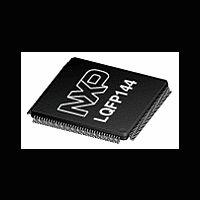
LPC2926_27_29 NXP Semiconductors, LPC2926_27_29 Datasheet - Page 33

LPC2926_27_29
Manufacturer Part Number
LPC2926_27_29
Description
The LPC2926/2927/2929 combine an ARM968E-S CPU core with two integrated TCMblocks operating at frequencies of up to 125 MHz, Full-speed USB 2
Manufacturer
NXP Semiconductors
Datasheet
1.LPC2926_27_29.pdf
(95 pages)
- Current page: 33 of 95
- Download datasheet (2Mb)
NXP Semiconductors
LPC2926_27_29
Product data sheet
6.13.4.1 Pin description
6.13.4.2 Clock description
6.13.4 UARTs
6.13.5 Serial Peripheral Interface (SPI)
The LPC2926/2927/2929 contains two identical UARTs located at different peripheral
base addresses. The key features are:
The UART is commonly used to implement a serial interface such as RS232. The
LPC2926/2927/2929 contains two industry-standard 550 UARTs with 16-byte transmit and
receive FIFOs, but they can also be put into 450 mode without FIFOs.
Remark: The LIN controller can be configured to provide two additional standard UART
interfaces (see
The UART pins are combined with other functions on the port pins of the
LPC2926/2927/2929.
Table 17.
The UART modules are clocked by two different clocks; CLK_SYS_PESS and
CLK_UARTx (x = 0 to 1), see
CLK_UARTx branch clock for power management. The frequency of all CLK_UARTx
clocks is identical since they are derived from the same base clock BASE_CLK_UART.
The register interface towards the system bus is clocked by CLK_SYS_PESS. The baud
generator is clocked by the CLK_UARTx.
The LPC2926/2927/2929 contains three Serial Peripheral Interface modules (SPIs) to
allow synchronous serial communication with slave or master peripherals.
The key features are:
Symbol
UARTx TXD
UARTx RXD
•
•
•
•
•
•
•
•
•
•
16-byte receive and transmit FIFOs.
Register locations conform to 550 industry standard.
Receiver FIFO trigger points at 1 byte, 4 bytes, 8 bytes and 14 bytes.
Built-in baud rate generator.
Support for RS-485/9-bit mode allows both software address detection and automatic
address detection using 9-bit mode.
Master or slave operation.
Each SPI supports up to four slaves in sequential multi-slave operation.
Supports timer-triggered operation.
Programmable clock bit rate and prescale based on SPI source clock
(BASE_SPI_CLK), independent of system clock.
Separate transmit and receive FIFO memory buffers; 16 bits wide, 32 locations deep.
UART pins
TXDx
RXDx
Pin name
Section
All information provided in this document is subject to legal disclaimers.
Rev. 5 — 28 September 2010
Table 17
6.14.2).
OUT
IN
Direction
Section
shows the UART pins (x runs from 0 to 1).
6.7.2. Note that each UART has its own
ARM9 microcontroller with CAN, LIN, and USB
UART channel x transmit data output
UART channel x receive data input
Description
LPC2926/2927/2929
© NXP B.V. 2010. All rights reserved.
33 of 95
Related parts for LPC2926_27_29
Image
Part Number
Description
Manufacturer
Datasheet
Request
R
Part Number:
Description:
Lpc2926/2927/2929 Arm9 Microcontroller With Can, Lin, And Usb
Manufacturer:
NXP Semiconductors
Datasheet:
Part Number:
Description:
NXP Semiconductors designed the LPC2420/2460 microcontroller around a 16-bit/32-bitARM7TDMI-S CPU core with real-time debug interfaces that include both JTAG andembedded trace
Manufacturer:
NXP Semiconductors
Datasheet:

Part Number:
Description:
NXP Semiconductors designed the LPC2458 microcontroller around a 16-bit/32-bitARM7TDMI-S CPU core with real-time debug interfaces that include both JTAG andembedded trace
Manufacturer:
NXP Semiconductors
Datasheet:
Part Number:
Description:
NXP Semiconductors designed the LPC2468 microcontroller around a 16-bit/32-bitARM7TDMI-S CPU core with real-time debug interfaces that include both JTAG andembedded trace
Manufacturer:
NXP Semiconductors
Datasheet:
Part Number:
Description:
NXP Semiconductors designed the LPC2470 microcontroller, powered by theARM7TDMI-S core, to be a highly integrated microcontroller for a wide range ofapplications that require advanced communications and high quality graphic displays
Manufacturer:
NXP Semiconductors
Datasheet:
Part Number:
Description:
NXP Semiconductors designed the LPC2478 microcontroller, powered by theARM7TDMI-S core, to be a highly integrated microcontroller for a wide range ofapplications that require advanced communications and high quality graphic displays
Manufacturer:
NXP Semiconductors
Datasheet:
Part Number:
Description:
The Philips Semiconductors XA (eXtended Architecture) family of 16-bit single-chip microcontrollers is powerful enough to easily handle the requirements of high performance embedded applications, yet inexpensive enough to compete in the market for hi
Manufacturer:
NXP Semiconductors
Datasheet:
Part Number:
Description:
The XA-S3 device is a member of Philips Semiconductors? XA(eXtended Architecture) family of high performance 16-bitsingle-chip microcontrollers
Manufacturer:
NXP Semiconductors
Datasheet:

Part Number:
Description:
The NXP BlueStreak LH75401/LH75411 family consists of two low-cost 16/32-bit System-on-Chip (SoC) devices
Manufacturer:
NXP Semiconductors
Datasheet:

Part Number:
Description:
The NXP LPC3130/3131 combine an 180 MHz ARM926EJ-S CPU core, high-speed USB2
Manufacturer:
NXP Semiconductors
Datasheet:

Part Number:
Description:
The NXP LPC3141 combine a 270 MHz ARM926EJ-S CPU core, High-speed USB 2
Manufacturer:
NXP Semiconductors

Part Number:
Description:
The NXP LPC3143 combine a 270 MHz ARM926EJ-S CPU core, High-speed USB 2
Manufacturer:
NXP Semiconductors

Part Number:
Description:
The NXP LPC3152 combines an 180 MHz ARM926EJ-S CPU core, High-speed USB 2
Manufacturer:
NXP Semiconductors

Part Number:
Description:
The NXP LPC3154 combines an 180 MHz ARM926EJ-S CPU core, High-speed USB 2
Manufacturer:
NXP Semiconductors


