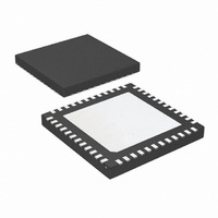
DS16EV5110ASQE/NOPB National Semiconductor, DS16EV5110ASQE/NOPB Datasheet - Page 15

DS16EV5110ASQE/NOPB
Manufacturer Part Number
DS16EV5110ASQE/NOPB
Description
IC EQUALIZER VIDEO 3D+C 48LLP
Manufacturer
National Semiconductor
Type
Video Equalizerr
Datasheet
1.DS16EV5110ASQXNOPB.pdf
(20 pages)
Specifications of DS16EV5110ASQE/NOPB
Applications
HD Displays, DVI/HDMI
Mounting Type
Surface Mount
Package / Case
48-LLP
Supply Voltage Range
3V To 3.6V
Operating Temperature Range
-40°C To +85°C
Digital Ic Case Style
LLP
No. Of Pins
48
Msl
MSL 3 - 168 Hours
Filter Terminals
SMD
No. Of I/o's
8
Rohs Compliant
Yes
Communication Function
Multi-Channel Equalizer
Lead Free Status / RoHS Status
Lead free / RoHS Compliant
Other names
DS16EV5110ASQETR
Available stocks
Company
Part Number
Manufacturer
Quantity
Price
General Recommendations
The DS16EV5110A is a high performance circuit capable of
delivering excellent performance. Careful attention must be
paid to the details associated with high-speed design as well
as providing a clean power supply. Refer to the LVDS
Owner’s Manual for more detailed information on high-speed
design tips as well as many other available resources avail-
able addressing signal integrity design issues.
PCB LAYOUT CONSIDERATIONS FOR DIFFERENTIAL
PAIRS
The TMDS differential inputs and outputs must have a con-
trolled differential impedance of 100Ω. It is preferable to route
TMDS lines exclusively on one layer of the board, particularly
for the input traces. The use of vias should be avoided if pos-
sible. If vias must be used, they should be used sparingly and
must be placed symmetrically for each side of a given differ-
ential pair. Route the TMDS signals away from other signals
and noise sources on the printed circuit board. All traces of
TMDS differential inputs and outputs must be equal in length
to minimize intra-pair skew.
LLP FOOTPRINT RECOMMENDATIONS
See National application note: AN-1187 for additional infor-
mation on LLP packages footprint and soldering information.
FIGURE 11. Equivalent CML Output Structure
FIGURE 12. Equivalent CML Input Structure
15
POWER SUPPLY BYPASSING
Two approaches are recommended to ensure that the
DS16EV5110A is provided with an adequate power supply.
First, the supply (VDD) and ground (GND) pins should be
connected to power planes routed on adjacent layers of the
printed circuit board. The layer thickness of the dielectric
should be minimized so that the VDD and GND planes create
a low inductance supply with distributed capacitance. Sec-
ond, careful attention to supply bypassing through the proper
use of bypass capacitors is required. A 0.1µF bypass capac-
itor should be connected to each VDD pin such that the
capacitor
DS16EV5110A. Smaller body size capacitors can help facili-
tate proper component placement. Additionally, three capac-
itors with capacitance in the range of 2.2µF to 10µF should
be incorporated in the power supply bypassing design as well.
These capacitors can be either tantalum or an ultra-low ESR
ceramic and should be placed as close as possible to the
DS16EV5110A.
EQUIVALENT I/O STRUCTURES
Figure 11 shows the DS16EV5110A CML output structure
and ESD protection circuitry.
Figure 12 shows the DS16EV5110A CML input structure and
ESD protection circuitry.
is
30064640
placed
30064641
as
close
as
possible
www.national.com
to
the


