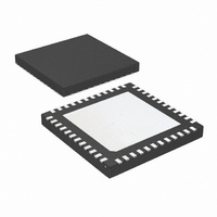
DS16EV5110ASQE/NOPB National Semiconductor, DS16EV5110ASQE/NOPB Datasheet - Page 5

DS16EV5110ASQE/NOPB
Manufacturer Part Number
DS16EV5110ASQE/NOPB
Description
IC EQUALIZER VIDEO 3D+C 48LLP
Manufacturer
National Semiconductor
Type
Video Equalizerr
Datasheet
1.DS16EV5110ASQXNOPB.pdf
(20 pages)
Specifications of DS16EV5110ASQE/NOPB
Applications
HD Displays, DVI/HDMI
Mounting Type
Surface Mount
Package / Case
48-LLP
Supply Voltage Range
3V To 3.6V
Operating Temperature Range
-40°C To +85°C
Digital Ic Case Style
LLP
No. Of Pins
48
Msl
MSL 3 - 168 Hours
Filter Terminals
SMD
No. Of I/o's
8
Rohs Compliant
Yes
Communication Function
Multi-Channel Equalizer
Lead Free Status / RoHS Status
Lead free / RoHS Compliant
Other names
DS16EV5110ASQETR
Available stocks
Company
Part Number
Manufacturer
Quantity
Price
t
t
OUTPUT JITTER
TJ1
TJ2
TJ3
TJ4
RJ
BIT RATE
F
BR
CCSK
D
CLK
Note 1: “Absolute Maximum Ratings” indicate limits beyond which damage to the device may occur, including inoperability and degradation of device reliability
and/or performance. Functional operation of the device and/or non-degradation at the Absolute Maximum Ratings or other conditions beyond those indicated in
the Recommended Operating Conditions is not implied. The Recommended Operating Conditions indicate conditions at which the device is functional and the
device should not be operated beyond such conditions. Absolute Maximum Numbers are guaranteed for a junction temperature range of –40°C to +125°C. Models
are validated to Maximum Operating Voltages only.
Note 2: Typical values represent most likely parametric norms at V
characterization and are not guaranteed.
Note 3: The Electrical Characteristics tables list guaranteed specifications under the listed Recommended Operating Conditions except as otherwise modified
or specified by the Electrical Characteristics Conditions and/or Notes.
Note 4: Allowed supply noise (mV
Note 5: Specification is guaranteed by characterization and is not tested in production.
Note 6: Deterministic jitter is measured at the differential outputs (TPC of Figure 2), minus the deterministic jitter before the test channel (TPA of Figure 2). Random
jitter is removed through the use of averaging or similar means.
Note 7: Total Jitter is defined as peak-to-peak deterministic jitter from (Note 8) + 14.2 times random jitter in ps
Note 8: Random jitter contributed by the equalizer is defined as sq rt (J
J
Symbol
IN
is the random jitter at the input of the equalizer in ps
Inter Pair Channel-to-Channel
Skew (all 4 Channels)
Latency
Total Jitter at 1.65 Gbps
Total Jitter at 2.25 Gbps
Total Jitter at 165 MHz
Total Jitter at 225 MHz
Random Jitter
Clock Frequency
Bit Rate
Parameter
P-P
sine wave) under typical conditions.
rms
, see TPA of Figure 2.
Difference in 50% crossing
between shortest and longest
channels
20m 28 AWG STP DVI Cable
Data Paths
EQ Setting 0x04 PRBS7
(Notes 5, 6, 7)
20m 28 AWG STP DVI Cable
Data Paths
EQ Setting 0x04 PRBS7
(Notes 5, 6, 7)
Clock Paths
Clock Pattern
(Notes 5, 6, 7)
Clock Paths
Clock Pattern
(Notes 5, 6, 7)
(Notes 7, 8)
Clock Path
(Note 5)
Data Path
(Note 5)
DD
= 3.3V, T
OUT
Conditions
2
− J
5
A
IN
2
= 25°C, and at the Recommended Operation Conditions at the time of product
). J
OUT
is the random jitter at equalizer outputs in ps
0.25
Min
25
rms
.
0.165
0.13
Typ
350
0.2
25
3
rms
, see TPC of Figure 2;
0.165
Max
0.17
2.25
225
www.national.com
Units
Gbps
UI
UI
UI
UI
ps
MHz
ps
ps
P-P
P-P
P-P
P-P
rms


