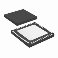
DS16EV5110ASQE/NOPB National Semiconductor, DS16EV5110ASQE/NOPB Datasheet - Page 2

DS16EV5110ASQE/NOPB
Manufacturer Part Number
DS16EV5110ASQE/NOPB
Description
IC EQUALIZER VIDEO 3D+C 48LLP
Manufacturer
National Semiconductor
Type
Video Equalizerr
Datasheet
1.DS16EV5110ASQXNOPB.pdf
(20 pages)
Specifications of DS16EV5110ASQE/NOPB
Applications
HD Displays, DVI/HDMI
Mounting Type
Surface Mount
Package / Case
48-LLP
Supply Voltage Range
3V To 3.6V
Operating Temperature Range
-40°C To +85°C
Digital Ic Case Style
LLP
No. Of Pins
48
Msl
MSL 3 - 168 Hours
Filter Terminals
SMD
No. Of I/o's
8
Rohs Compliant
Yes
Communication Function
Multi-Channel Equalizer
Lead Free Status / RoHS Status
Lead free / RoHS Compliant
Other names
DS16EV5110ASQETR
Available stocks
Company
Part Number
Manufacturer
Quantity
Price
www.national.com
HIGH SPEED DIFFERENTIAL I/O
C_IN−
C_IN+
D_IN0−
D_IN0+
D_IN1−
D_IN1+
D_IN2−
D_IN2+
C_OUT-
C_OUT+
D_OUT0−
D_OUT0+
D_OUT1–
D_OUT1+
D_OUT2−
D_OUT2+
Equalization Control
BST_0
BST_1
BST_2
Device Control
EN
FEB
SD
POWER
V
GND
Exposed
Pad
System Management Bus (SMBus) Interface Control Pins
SDA
SDC
CS
Other
Reserv
Pin Name
DD
Pin Descriptions
Note: I = Input, O = Output,
Pin Number
19, 20, 38,
42, 43, 47,
39, 40,41,
3, 6, 7,
10, 13,
22, 24,
27, 30,
15, 46
31, 34
DAP
11
12
36
35
33
32
29
28
26
25
23
14
37
44
21
45
18
17
16
48
1
2
4
5
8
9
IO =Input/Output,
O, LVCMOS Equalizer Clock Channel Signal Detect Output. Produces a High when signal is detected.
I, LVCMOS BST_0, BST_1, and BST_2 select the equalizer boost level for EQ channels. BST_0,
I, LVCMOS Enable Equalizer input. When held High, normal operation is selected. When held Low,
I, LVCMOS Force External Boost. When held High, the equalizer boost setting is controlled by the BST_
I, LVCMOS SMBus Clock Input. Internally pulled High to 3.3V with High-Z pull up.
I, LVCMOS SMBus Chip select. When held High, the equalizer SMBus register is enabled. When held
I/O, Type
LVCMOS
O, CML
O, CML
O, CML
O, CML
I, CML
I, CML
I, CML
I, CML
Power
GND
GND
IO,
Inverting and non-inverting TMDS Clock inputs to the equalizer. An on-chip 50Ω terminating
resistor connects C_IN+ to VDD and C_IN- to VDD.
Inverting and non-inverting TMDS Data inputs to the equalizer. An on-chip 50Ω terminating
resistor connects D_IN0+ to VDD and D_IN0- to VDD.
Inverting and non-inverting TMDS Data inputs to the equalizer. An on-chip 50Ω terminating
resistor connects D_IN1+ to VDD and D_IN1- to VDD.
Inverting and non-inverting TMDS Data inputs to the equalizer. An on-chip 50Ω terminating
resistor connects D_IN2+ to VDD and D_IN2- to VDD.
Inverting and non-inverting TMDS outputs from the equalizer. Open collector.
Inverting and non-inverting TMDS outputs from the equalizer. Open collector.
Inverting and non-inverting TMDS outputs from the equalizer. Open collector.
Inverting and non-inverting TMDS outputs from the equalizer. Open collector.
BST_1, and BST_2 are internally pulled Low. See Table 2.
standby mode is selected. EN is internally pulled High. Signal is global to all Data and Clock
channels.
[0:2] pins. When held Low, the equalizer boost level is controlled through the SMBus (see
Table 1) control pins. FEB is internally pulled High.
V
capacitor should be connected between each V
Ground reference. GND should be tied to a solid ground plane through a low impedance
path.
The exposed pad at the center of the package must be connected to the ground plane.
SMBus Data Input / Output. Internally pulled High to 3.3V with High-Z pull up.
Low, the equalizer SMBus register is disabled. CS is internally pulled Low. CS is internally
gated with SDC.
Reserved. Do not connect.
DD
pins should be tied to the V
2
DD
plane through a low inductance path. A 0.1µF bypass
Description
DD
pin to the GND planes.


