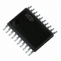
74LVT245PW,112 NXP Semiconductors, 74LVT245PW,112 Datasheet - Page 4

74LVT245PW,112
Manufacturer Part Number
74LVT245PW,112
Description
IC TRANSCVR TRI-ST 8BIT 20TSSOP
Manufacturer
NXP Semiconductors
Series
74LVTr
Datasheet
1.74LVT245DB118.pdf
(15 pages)
Specifications of 74LVT245PW,112
Logic Type
Transceiver, Non-Inverting
Package / Case
20-TSSOP
Number Of Elements
1
Number Of Bits Per Element
8
Current - Output High, Low
32mA, 64mA
Voltage - Supply
2.7 V ~ 3.6 V
Operating Temperature
-40°C ~ 85°C
Mounting Type
Surface Mount
Logic Family
74LVT
Number Of Channels Per Chip
8
Input Level
LVTTL
Output Level
LVTTL
Output Type
3-State
High Level Output Current
- 32 mA
Low Level Output Current
64 mA
Propagation Delay Time
2.4 ns
Supply Voltage (max)
3.6 V
Supply Voltage (min)
2.7 V
Maximum Operating Temperature
+ 85 C
Function
Bus Transceiver
Input Bias Current (max)
12000 uA
Minimum Operating Temperature
- 40 C
Mounting Style
SMD/SMT
Polarity
Non-Inverting
Number Of Circuits
8
Lead Free Status / RoHS Status
Lead free / RoHS Compliant
Lead Free Status / RoHS Status
Lead free / RoHS Compliant, Lead free / RoHS Compliant
Other names
568-1595-5
74LVT245PW
935175550112
74LVT245PW
935175550112
NXP Semiconductors
6. Functional description
Table 3.
[1]
7. Limiting values
Table 4.
In accordance with the Absolute Maximum Rating System (IEC 60134). Voltages are referenced to GND (ground = 0 V).
[1]
[2]
[3]
[4]
8. Recommended operating conditions
Table 5.
74LVT245_3
Product data sheet
Inputs
OE
L
L
H
Symbol
V
V
V
I
I
I
T
T
P
Symbol
V
V
I
IK
OK
O
OH
stg
j
CC
I
O
tot
CC
I
H = HIGH voltage level;
L = LOW voltage level;
X = don’t care;
Z = high impedance OFF-state.
Stresses beyond those listed may cause permanent damage to the device. These are stress ratings only and functional operation of the
device at these or any other conditions beyond those indicated under “recommended operating conditions” is not implied. Exposure to
absolute-maximum-rated conditions for extended periods may affect device reliability.
The performance capability of a high-performance integrated circuit in conjunction with its thermal environment can create junction
temperatures which are detrimental to reliability. The maximum junction temperature of this integrated circuit should not exceed 150 C.
The input and output negative voltage ratings may be exceeded if the input and output clamp current ratings are observed.
For SO20 packages: above 70 C derate linearly with 8 mW/K.
For SSOP20 and TSSOP20 packages: above 60 C derate linearly with 5.5 mW/K.
For DHVQFN20 packages: above 60 C derate linearly with 4.5 mW/K.
Parameter
supply voltage
input voltage
HIGH-level output current
Function selection
Limiting values
Recommended operating conditions
Parameter
supply voltage
input voltage
output voltage
input clamping current
output clamping current
output current
storage temperature
junction temperature
total power dissipation
DIR
L
H
X
Conditions
output in OFF or HIGH state
V
V
output in LOW state
output in HIGH state
T
amb
I
O
Conditions
< 0 V
< 0 V
= 40 C to +85 C
Rev. 03 — 8 May 2008
Inputs/outputs
An
An = Bn
inputs
Z
3.3 V octal transceiver with direction pin (3-state)
[3]
[3]
[4]
Min
-
-
-
0.5
0.5
0.5
50
50
64
65
Min
2.7
0
-
Bn
inputs
Bn = An
Z
Max
+4.6
7.0
+7
-
-
128
-
+150
+150
500
74LVT245
© NXP B.V. 2008. All rights reserved.
Max
3.6
5.5
32
Unit
V
V
V
mA
mA
mA
mA
mW
C
C
Unit
V
V
mA
4 of 15
[1][2]


