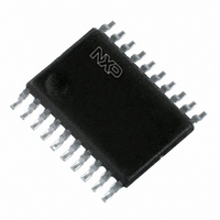
74LVT245PW,112 NXP Semiconductors, 74LVT245PW,112 Datasheet - Page 6

74LVT245PW,112
Manufacturer Part Number
74LVT245PW,112
Description
IC TRANSCVR TRI-ST 8BIT 20TSSOP
Manufacturer
NXP Semiconductors
Series
74LVTr
Datasheet
1.74LVT245DB118.pdf
(15 pages)
Specifications of 74LVT245PW,112
Logic Type
Transceiver, Non-Inverting
Package / Case
20-TSSOP
Number Of Elements
1
Number Of Bits Per Element
8
Current - Output High, Low
32mA, 64mA
Voltage - Supply
2.7 V ~ 3.6 V
Operating Temperature
-40°C ~ 85°C
Mounting Type
Surface Mount
Logic Family
74LVT
Number Of Channels Per Chip
8
Input Level
LVTTL
Output Level
LVTTL
Output Type
3-State
High Level Output Current
- 32 mA
Low Level Output Current
64 mA
Propagation Delay Time
2.4 ns
Supply Voltage (max)
3.6 V
Supply Voltage (min)
2.7 V
Maximum Operating Temperature
+ 85 C
Function
Bus Transceiver
Input Bias Current (max)
12000 uA
Minimum Operating Temperature
- 40 C
Mounting Style
SMD/SMT
Polarity
Non-Inverting
Number Of Circuits
8
Lead Free Status / RoHS Status
Lead free / RoHS Compliant
Lead Free Status / RoHS Status
Lead free / RoHS Compliant, Lead free / RoHS Compliant
Other names
568-1595-5
74LVT245PW
935175550112
74LVT245PW
935175550112
NXP Semiconductors
Table 6.
At recommended operating conditions. Voltages are referenced to GND (ground = 0 V).
[1]
[2]
[3]
[4]
[5]
10. Dynamic characteristics
Table 7.
Voltages are referenced to GND (ground = 0 V). For test circuit see
74LVT245_3
Product data sheet
Symbol Parameter
I
C
C
Symbol Parameter
t
t
t
t
t
CC
PLH
PHL
PZH
PZL
PHZ
I
I
I/O
CC
All typical values are measured at V
Unused pins at V
This parameter is valid for any V
a transition time of 100 ms is permitted. This parameter is valid for T
This is the bus hold overdrive current required to force the input to the opposite logic state.
This is the increase in supply current for each input at the specified voltage level other than V
LOW to HIGH propagation delay
HIGH to LOW propagation delay
OFF-state to HIGH propagation delay see
OFF-state to LOW propagation delay see
HIGH to OFF-state propagation delay see
supply current
additional supply current
input capacitance
input/output capacitance
Static characteristics
Dynamic characteristics
CC
or GND.
CC
…continued
between 0 V and 1.2 V with a transition time of up to 10 ms. From V
CC
= 3.3 V (unless stated otherwise) and T
Conditions
V
per input pin; V
one input = V
other inputs at V
DIR and OE inputs; outputs disabled;
V
at input/output data pins, outputs disabled;
V
CC
I
I/O
outputs HIGH
outputs LOW
outputs disabled
= 0 V or 3.0 V
= 0 V or 3.0 V
= 3.6 V; V
Conditions
An to Bn or Bn to An
An to Bn or Bn to An
V
V
V
V
V
V
V
V
V
V
Rev. 03 — 8 May 2008
CC
CC
CC
CC
CC
CC
CC
CC
CC
CC
CC
Figure 6
Figure 6
Figure 6
I
CC
= V
CC
= 2.7 V
= 3.3 V
= 2.7 V
= 3.3 V
= 2.7 V
= 3.3 V
= 2.7 V
= 3.3 V
= 2.7 V
= 3.3 V
= 3.0 V to 3.6 V;
0.6 V;
CC
or GND
or GND; I
amb
3.3 V octal transceiver with direction pin (3-state)
0.3 V
0.3 V
0.3 V
0.3 V
0.3 V
Figure
= +25 C only.
O
= 0 A
amb
7.
= 25 C.
[5]
CC
or GND.
Min
Min
1.0
1.0
1.1
1.1
2.2
-
-
-
-
-
-
-
-
-
-
-
CC
40 C to +85 C
40 C to +85 C
= 1.2 V to V
Typ
2.4
2.4
3.3
3.3
3.6
Typ
74LVT245
0.13
0.13
-
-
-
-
-
0.1
10
3
4
[1]
© NXP B.V. 2008. All rights reserved.
[1]
CC
Max
= 3.3 V
4.7
4.0
4.6
4.0
7.1
5.5
6.5
5.5
6.5
5.9
Max
0.19
0.19
0.2
12
-
-
Unit
ns
ns
ns
ns
ns
ns
ns
ns
ns
ns
6 of 15
Unit
mA
mA
mA
mA
pF
pF
0.3 V


