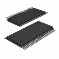
74ALVT162827DGG,11 NXP Semiconductors, 74ALVT162827DGG,11 Datasheet - Page 5

74ALVT162827DGG,11
Manufacturer Part Number
74ALVT162827DGG,11
Description
IC BUFF DVR TRI-ST 20BIT 56TSSOP
Manufacturer
NXP Semiconductors
Series
74ALVTr
Datasheet
1.74ALVT162827DGG11.pdf
(10 pages)
Specifications of 74ALVT162827DGG,11
Logic Type
Buffer/Line Driver, Non-Inverting
Number Of Elements
2
Number Of Bits Per Element
10
Current - Output High, Low
8mA, 12mA
Voltage - Supply
2.3 V ~ 2.7 V
Operating Temperature
-40°C ~ 85°C
Mounting Type
Surface Mount
Package / Case
56-TSSOP
Logic Family
ALVT
Number Of Channels Per Chip
20
Polarity
Non-Inverting
Supply Voltage (max)
3.6 V
Supply Voltage (min)
2.3 V
Maximum Operating Temperature
+ 85 C
Mounting Style
SMD/SMT
High Level Output Current
- 12 mA
Low Level Output Current
12 mA
Minimum Operating Temperature
- 40 C
Number Of Lines (input / Output)
20 / 20
Output Type
3-State
Propagation Delay Time
2.7 ns at 2.5 V, 2.2 ns at 3.3 V
Lead Free Status / RoHS Status
Lead free / RoHS Compliant
Other names
74ALVT162827DG
74ALVT162827DG
935210070112
74ALVT162827DG
935210070112
1. All typical values are at V
2. This is the increase in supply current for each input at the specified voltage level other than V
3. This parameter is valid for any V
4. Unused pins at V
5. I
6. This is the bus hold overdrive current required to force the input to the opposite logic state.
Philips Semiconductors
DC ELECTRICAL CHARACTERISTICS (3.3V "0.3V RANGE)
NOTES:
AC CHARACTERISTICS (3.3V "0.3V RANGE)
GND = 0V, t
1998 Feb 13
SYMBOL
t
t
t
t
t
t
PLH
PHL
PZH
PZL
PHZ
PLZ
2.5V/3.3V 20-bit buffer/line driver, non-inverting,
with 30 termination resistors (3-State)
SYMBOL
I
transition time of 100 sec is permitted. This parameter is valid for T
I
PU/PD
HOLD
I
I
CCZ
V
I
I
I
I
V
V
OFF
I
OZH
CCH
CCL
CCZ
OZL
EX
I
OH
OL
I
I
CC
IK
I
I
is measured with outputs pulled up to V
R
Input clamp voltage
High-level output voltage
Low–level output voltage
Input leakage current
In ut leakage current
Off current
Bus Hold current
Bus Hold current
Data inputs
Data in uts
Current into an output in the
High state when V
Power up/down 3-State output
current
3-State output High current
3-State output Low current
Quiescent supply current
Additional supply current per
input pin
= t
F
Propagation delay
nAx to nYx
Output enable time
to High and Low level
Output disable time
from High and Low level
= 2.5ns, C
CC
3
2
PARAMETER
or GND.
6
PARAMETER
CC
L
= 50pF, R
= 3.3V and T
O
> V
CC
CC
between 0V and 1.2V with a transition time of up to 10msec. From V
L
= 500
amb
CC
V
V
V
V
V
V
V
V
V
V
V
V
V
V
V
OE/OE = Don’t care
V
V
V
V
V
V
Other inputs at V
= 25 C.
CC
CC
CC
CC
CC
CC
CC
CC
CC
CC
CC
CC
CC
O
CC
CC
CC
CC
CC
CC
CC
or pulled down to ground.
= 5.5V; V
= 3.0V; I
= 3.0V; I
= 3.0V; I
= 3.6V; V
= 0 or 3 6V; V
= 0 or 3.6V; V
= 3 6V; V
= 3.6V; V
= 3.6V; V
= 0V; V
= 3V; V
= 3V; V
= 0V to 3.6V; V
= 3.6V; V
= 3.6V; V
= 3.6V; Outputs High, V
= 3.6V; Outputs Low, V
= 3.6V; Outputs Disabled; V
= 3V to 3.6V; One input at V
1.2V; V
I
I
I
CC
IK
OH
OL
or V
= 0.8V
= 2.0V
O
I
I
I
I
O
O
WAVEFORM
= V
= V
= V
= 0
= –18mA
= 0.5V to V
= 3.0V
= 3.0V; V
= 0.5V; V
= 12mA
= –12mA
CC
O
TEST CONDITIONS
I
I
CC
CC
CC
= 0 to 4.5V
= 5 5V
= 5.5V
CC
or GND
1
2
2
or GND
= 3.6V
5
amb
I
I
= V
= V
CC
I
= 25 C only.
I
= GND or V
= GND or V
; V
IL
IL
or V
or V
I
I
CC
= GND or V
= GND or V
–0.6V,
IH
IH
CC,
CC,
MIN
Control pins
1.0
1.0
1.5
1.0
1.5
1.0
Data pins
Data ins
I
I
O =
CC
CC,
O =
CC
T
0
0
I
V
amb
O =
CC
or GND
4
4
4
0
= -40 to +85
= +3.3V 0.3V
5
LIMITS
TYP
2.2
2.0
3.4
2.4
3.4
2.7
CC
Temp = -40 C to +85 C
MIN
–75
2.0
75
500
= 1.2V to V
74ALVT162827
o
C
LIMITS
MAX
–0.85
TYP
–140
0.07
0.07
0.04
3.3
3.0
5.6
3.7
5.2
4.5
130
2.3
0.5
0.1
0 1
0.1
0 5
0.5
0.1
0.1
0.5
0.5
3.9
10
1
CC
1
Product specification
= 3.3V
MAX
–1.2
125
0.8
0.1
5.5
0.1
0.4
10
10
100
100
–5
-5
1
1
5
1
UNIT
0.3V a
ns
ns
ns
UNIT
mA
mA
V
V
V
A
A
A
A
A
A
A
A
A
A


