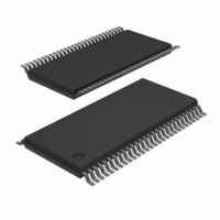
74ALVT162827DGG,11 NXP Semiconductors, 74ALVT162827DGG,11 Datasheet - Page 7

74ALVT162827DGG,11
Manufacturer Part Number
74ALVT162827DGG,11
Description
IC BUFF DVR TRI-ST 20BIT 56TSSOP
Manufacturer
NXP Semiconductors
Series
74ALVTr
Datasheet
1.74ALVT162827DGG11.pdf
(10 pages)
Specifications of 74ALVT162827DGG,11
Logic Type
Buffer/Line Driver, Non-Inverting
Number Of Elements
2
Number Of Bits Per Element
10
Current - Output High, Low
8mA, 12mA
Voltage - Supply
2.3 V ~ 2.7 V
Operating Temperature
-40°C ~ 85°C
Mounting Type
Surface Mount
Package / Case
56-TSSOP
Logic Family
ALVT
Number Of Channels Per Chip
20
Polarity
Non-Inverting
Supply Voltage (max)
3.6 V
Supply Voltage (min)
2.3 V
Maximum Operating Temperature
+ 85 C
Mounting Style
SMD/SMT
High Level Output Current
- 12 mA
Low Level Output Current
12 mA
Minimum Operating Temperature
- 40 C
Number Of Lines (input / Output)
20 / 20
Output Type
3-State
Propagation Delay Time
2.7 ns at 2.5 V, 2.2 ns at 3.3 V
Lead Free Status / RoHS Status
Lead free / RoHS Compliant
Other names
74ALVT162827DG
74ALVT162827DG
935210070112
74ALVT162827DG
935210070112
Philips Semiconductors
AC WAVEFORMS
V
V
V
TEST CIRCUIT AND WAVEFORM
1998 Feb 13
nYx
OUTPUT
M
X
Y
nAx INPUT
Waveform 1. Input (nAx) to Output (nYx) Propagation Delays
2.5V/3.3V 20-bit buffer/line driver, non-inverting,
with 30 termination resistors (3-State)
= V
= V
= 1.5V for V
GENERATOR
DEFINITIONS
R
C
R
SWITCH POSITION
t
t
t
L
L
T
PHZ
PLH/
PLZ/
OL
OH
PULSE
TEST
= Load resistor; see AC CHARACTERISTICS for value.
= Load capacitance includes jig and probe capacitance:
= Termination resistance should be equal to Z
+ 0.3V for V
/t
– 0.3V for V
t
t
PZL
PHL
PZH
See AC CHARACTERISTICS for value.
pulse generators.
CC
V
SWITCH
M
Test Circuit for 3-State Outputs
t
w 3.0V; V
PLH
Open
6V or V
GND
V
IN
CC
CC
R
w 3.0V; V
w 3.0V; V
V
T
M
CC x 2
M
= V
D.U.T.
CC
V
X
Y
CC
= V
/2 for V
= V
OL
OH
V
M
t
PHL
+ 0.15V for V
V
– 0.15V for V
CC
OUT
v 2.7V
C
L
V
M
OUT
CC
CC
3.0V or V
whichever
is less
0V
V
V
R
R
OH
OL
of
SA00016
L
L
v 2.7V
v 2.7V
6.0V or V
CC
GND
Open
7
CC
74ALVT16
FAMILY
x 2
nYx
OUTPUT
nYx
OUTPUT
NEGATIVE
PULSE
POSITIVE
PULSE
nOEx
INPUT
Waveform 2. 3-State Output Enable and Disable Times
90%
10%
3.0V or V
Amplitude
whichever
is less
V
V
M
M
t
V
t
PZH
V
PZL
M
= 1.5V or V
10%
90%
M
CC
INPUT PULSE REQUIREMENTS
t
t
THL
TLH
Input Pulse Definition
V
V
Rep. Rate
v10MHz
M
M
(t
(t
F
R
)
)
t
t
W
W
CC
/2 whichever is less
500ns
10%
90%
V
74ALVT162827
t
M
W
t
t
PLZ
PHZ
V
V
M
M
v2.5ns v2.5ns
Product specification
V
V
V
V
90%
10%
t
R
X
OL
OH
Y
t
t
TLH
THL
(t
(t
3.0V or V
whichever
0V
3.0V or V
0V
0V
V
0V
is less
SW00174
V
R
F
t
SW00025
IN
)
IN
)
F
CC
CC


