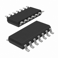
HEF4013BT,653 NXP Semiconductors, HEF4013BT,653 Datasheet - Page 7

HEF4013BT,653
Manufacturer Part Number
HEF4013BT,653
Description
IC FLIP FLOP DUAL DTYPE 14SOIC
Manufacturer
NXP Semiconductors
Series
4000Br
Type
D-Typer
Specifications of HEF4013BT,653
Package / Case
14-SOIC (3.9mm Width), 14-SOL
Function
Set(Preset) and Reset
Output Type
Differential
Number Of Elements
2
Number Of Bits Per Element
1
Frequency - Clock
40MHz
Trigger Type
Positive Edge
Current - Output High, Low
3.4mA, 3.4mA
Voltage - Supply
3 V ~ 15 V
Operating Temperature
-40°C ~ 125°C
Mounting Type
Surface Mount
Number Of Circuits
2
Logic Family
HEF4000
Logic Type
D-Type Edge Triggered Flip-Flop
Polarity
Inverting/Non-Inverting
Input Type
Single-Ended
Propagation Delay Time
30 ns at 15 V
High Level Output Current
- 4.2 mA
Low Level Output Current
4.2 mA
Supply Voltage (max)
15.5 V
Maximum Operating Temperature
+ 125 C
Mounting Style
SMD/SMT
Minimum Operating Temperature
- 40 C
Supply Voltage (min)
4.5 V
Lead Free Status / RoHS Status
Lead free / RoHS Compliant
Delay Time - Propagation
-
Lead Free Status / Rohs Status
Lead free / RoHS Compliant
Other names
933372660653
HEF4013BTD-T
HEF4013BTD-T
HEF4013BTD-T
HEF4013BTD-T
Available stocks
Company
Part Number
Manufacturer
Quantity
Price
Part Number:
HEF4013BT,653
Manufacturer:
NEXPERIA/安世
Quantity:
20 000
NXP Semiconductors
Table 7.
T
[1]
Table 8.
V
12. Waveforms
HEF4013B_6
Product data sheet
Symbol Parameter
t
f
Symbol Parameter
P
rec
clk(max)
amb
SS
Fig 4.
D
= 0 V; t
Typical values of the propagation delays and output transition times can be calculated with the extrapolation formulas. C
= 25 C; unless otherwise specified. For test circuit see
recovery time
maximum clock
frequency
Set-up and hold times are shown as positive values but may be specified as negative values.
The shaded areas indicate when the input is permitted to change for predictable output performance.
Measurement points are given in
Set-up time, hold time, minimum clock pulse width, propagation delays and transition times
dynamic power dissipation
r
Dynamic characteristics
input nCP
output nQ
Dynamic power dissipation
= t
input nD
f
20 ns; T
V
V
0 V
0 V
OH
OL
V
V
I
I
amb
= 25 C.
Conditions
nSD input;
see
nCD input;
see
see
V
M
Figure 5
Figure 5
Figure 4
…continued
V
V
10 V P
15 V P
Table
1/f
t
M
su
5 V P
DD
clk(max)
t
h
9.
t
PLH
Typical formula
D
D
D
Rev. 06 — 27 October 2009
= 850
= 3600
= 9000
V
V
X
V
M
Y
t
t
V
10 V
15 V
10 V
15 V
10 V
15 V
5 V
5 V
5 V
DD
f
i
f
f
+ (f
i
i
t
Figure
+ (f
W
+ (f
t
su
o
o
o
t
C
6.
h
C
Extrapolation formula Min
C
L
)
L
L
)
)
t
PHL
V
t
t
V
DD
V
DD
DD
2
t
f
2
2
W
W
W
Where
f
f
C
V
i
o
(f
DD
= input frequency in MHz;
L
= output frequency in MHz;
o
= output load capacitance in pF;
t
r
= supply voltage in V.
C
L
+15
) = sum of the outputs;
15
15
40
25
25
14
20
7
HEF4013B
Dual D-type flip-flop
Typ
© NXP B.V. 2009. All rights reserved.
25
10
10
14
28
40
001aah016
5
0
0
Max
-
-
-
-
-
-
-
-
-
L
is given in pF.
Unit
ns
ns
ns
ns
ns
ns
MHz
MHz
MHz
7 of 15


