74F794PC Fairchild Semiconductor, 74F794PC Datasheet
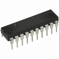
IC REGISTER READ-BACK 20-DIP

74F794PC

Manufacturer Part Number
74F794PC
Description
IC REGISTER READ-BACK 20-DIP
Manufacturer
Fairchild Semiconductor
Series
74Fr
Type
D-Type Busr
Datasheet

Specifications of 74F794PC

Function
Standard
Output Type
Tri-State Non Inverted
Number Of Elements
1
Number Of Bits Per Element
8
Frequency - Clock
90MHz
Delay Time - Propagation
2.5ns
Trigger Type
Positive Edge
Current - Output High, Low
15mA, 64mA
Voltage - Supply
4.5 V ~ 5.5 V
Operating Temperature
0°C ~ 70°C
Mounting Type
Through Hole
Package / Case
20-DIP (0.300", 7.62mm)
Lead Free Status / RoHS Status
Lead free / RoHS Compliant
Other names
74F794
© 2004 Fairchild Semiconductor Corporation
74F794PC
74F794
8-Bit Register with Readback
General Description
The 74F794 is an 8-bit register with readback capability
designed to store data as well as read the register informa-
tion back onto the data bus. The I/O bus (D bus) has
3-STATE outputs. Current sinking capability is 64 mA on
both the D and Q busses.
Data is loaded into the registers on the LOW-to-HIGH tran-
sition of the clock (CP). The output enable (OE) is used to
enable data on D
registers is enabled on D
bus. When OE is HIGH, D
configuring D as an input bus.
Ordering Code:
Logic Symbol
Order Number
0
–D
Package Number
7
. When OE is LOW, the output of the
N20A
0
0
–D
–D
7
7
, enabling D as an output
are inputs to the registers
20-Lead Plastic Dual-In-Line Package (PDIP), JEDEC MS-001, 0.300" Wide
DS010652
Features
Connection Diagram
3-STATE outputs on the I/O port
D and Q output sink capability of 64 mA
Functionally and pin equivalent to the 74LS794
Package Description
March 1990
Revised February 2004
www.fairchildsemi.com

Related parts for 74F794PC

74F794PC Summary of contents

Page 1

... input bus. Ordering Code: Order Number Package Number 74F794PC N20A 20-Lead Plastic Dual-In-Line Package (PDIP), JEDEC MS-001, 0.300" Wide Logic Symbol © 2004 Fairchild Semiconductor Corporation Features 3-STATE outputs on the I/O port D and Q output sink capability ...

Page 2

Input Loading/Fan-Out Pin Names OE Output Enable Input CP Clock Pulse Inputs D –D D Bus Inputs 3-STATE Outputs Q –Q Q Bus Outputs 0 7 Truth Table Inputs Outputs ...

Page 3

Absolute Maximum Ratings Storage Temperature Ambient Temperature under Bias Junction Temperature under Bias V Pin Potential to Ground Pin CC Input Voltage (Note 3) Input Current (Note 3) ESD Last Passing Voltage (Min) Voltage Applied to Output In HIGH State ...

Page 4

AC Electrical Characteristics Symbol Parameter f Maximum Clock Frequency MAX t Propagation Delay PLH PHL n t Output Enable Time PZH t PZL t Output Disable Time PHZ t PLZ t (H) Setup Time, HIGH or ...

Page 5

Physical Dimensions inches (millimeters) unless otherwise noted 20-Lead Plastic Dual-In-Line Package (PDIP), JEDEC MS-001, 0.300" Wide Fairchild does not assume any responsibility for use of any circuitry described, no circuit patent licenses are implied and Fairchild reserves the right at ...

Related keywords