74LV165DB,112 NXP Semiconductors, 74LV165DB,112 Datasheet - Page 4
74LV165DB,112
Manufacturer Part Number
74LV165DB,112
Description
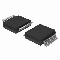
IC 8BIT SHIFT REGISTER 16SSOP
Manufacturer
NXP Semiconductors
Series
74LVr
Datasheet
1.74LV165N112.pdf
(14 pages)
Specifications of 74LV165DB,112
Logic Type
Shift Register
Output Type
Differential
Number Of Elements
1
Number Of Bits Per Element
8
Function
Parallel or Serial to Serial
Voltage - Supply
1 V ~ 5.5 V
Operating Temperature
-40°C ~ 125°C
Mounting Type
Surface Mount
Package / Case
16-SSOP
Lead Free Status / RoHS Status
Lead free / RoHS Compliant
Other names
74LV165DB
74LV165DB
935166030112
74LV165DB
935166030112


H =
h =
L =
I
q =
X =
1. The LV is guaranteed to function down to V
1. Stresses beyond those listed may cause permanent damage to the device. These are stress ratings only and functional operation of the
2. The input and output voltage ratings may be exceeded if the input and output current ratings are observed.
Philips Semiconductors
FUNCTION TABLE
NOTES:
RECOMMENDED OPERATING CONDITIONS
NOTE:
ABSOLUTE MAXIMUM RATINGS
In accordance with the Absolute Maximum Rating System (IEC 134).
Voltages are referenced to GND (ground = 0 V).
NOTES:
1998 May 07
Parallel load
Parallel load
Serial Shift
Serial Shift
Hold “do nothing”
SYMBOL
OPERATING MODES
OPERATING MODES
SYMBOL
8-bit parallel-in/serial-out shift register
"I
=
=
device at these or any other conditions beyond those indicated under “recommended operating conditions” is not implied. Exposure to
absolute-maximum-rated conditions for extended periods may affect device reliability.
T
V
"I
"I
P
t
"I
V
"I
V
amb
r
T
V
CC
, t
TOT
GND
stg
O
CC
I
OK
CC
f
IK
O
HIGH voltage level
HIGH voltage level one set-up time prior to the LOW-to-HIGH clock transition
LOW voltage level
LOW voltage level level one set-up time prior to the LOW-to-HIGH clock transition
lower case letters indicate the state of the referenced output one set-up time prior to the LOW-to-HIGH clock transition
don’t care
LOW-to-HIGH clock transition
,
DC supply voltage
Input voltage
Output voltage
Operating ambient temperature range in free air
Input rise and fall times
DC supply voltage
DC input diode current
DC output diode current
DC output source or sink current
– standard outputs
DC V
– standard outputs
Storage temperature range
Power dissipation per package
– plastic DIL
– plastic mini-pack (SO)
– plastic shrink mini-pack (SSOP and TSSOP)
CC
or GND current for types with
PARAMETER
PL
H
H
H
PARAMETER
L
L
1, 2
CE
CC
X
X
H
L
L
= 1.0V (input levels GND or V
INPUTS
CP
X
X
X
V
V
–0.5V < V
for temperature range: –40 to +125 C
above +70 C derate linearly with 12 mW/K
above +70 C derate linearly with 8 mW/K
above +60 C derate linearly with 5.5 mW/K
I
O
< –0.5 or V
< –0.5 or V
V
V
V
V
D
CC
CC
CC
CC
See DC and AC
X
X
X
4
h
characteristics
l
CONDITIONS
S
See Note 1
= 1.0V to 2.0V
= 2.0V to 2.7V
= 2.7V to 3.6V
= 3.6V to 5.5V
O
CC
< V
); DC characteristics are guaranteed from V
I
O
> V
CONDITIONS
CC
D
> V
0
CC
H
+ 0.5V
–D
L
X
X
X
CC
+ 0.5V
7
+ 0.5V
Qn REGISTERS
Q
q
H
H
L
L
MIN
0
–40
–40
0
1.0
0
0
–
–
–
–
Q
q
q
q
H–H
L–L
1
0
0
1–
TYP
–Q
–q
–q
3.3
q
–
–
–
–
–
–
5
5
6
6
–0.5 to +7.0
–65 to +150
RATING
750
500
400
CC
20
50
25
50
MAX
+125
Q
V
V
= 1.2V to V
q
q
q
+85
Product specification
500
200
100
H
5.5
L
50
6
6
7
CC
CC
7
74LV165
OUTPUTS
CC
UNIT
UNIT
ns/V
mW
mA
mA
mA
mA
Q
q
q
q
H
V
L
V
V
V
= 5.5V.
C
C
6
6
7
7
Related parts for 74LV165DB,112
Image
Part Number
Description
Manufacturer
Datasheet
Request
R

Part Number:
Description:
IC 8BIT SHIFT REGISTER 16SOIC
Manufacturer:
NXP Semiconductors
Datasheet:
Part Number:
Description:
IC 8BIT SHIFT REGISTER 16SOIC
Manufacturer:
NXP Semiconductors
Datasheet:

Part Number:
Description:
Counter Shift Registers 3.3V PARALLEL LOAD 8-BIT S/R
Manufacturer:
NXP Semiconductors
Part Number:
Description:
NXP Semiconductors designed the LPC2420/2460 microcontroller around a 16-bit/32-bitARM7TDMI-S CPU core with real-time debug interfaces that include both JTAG andembedded trace
Manufacturer:
NXP Semiconductors
Datasheet:

Part Number:
Description:
NXP Semiconductors designed the LPC2458 microcontroller around a 16-bit/32-bitARM7TDMI-S CPU core with real-time debug interfaces that include both JTAG andembedded trace
Manufacturer:
NXP Semiconductors
Datasheet:
Part Number:
Description:
NXP Semiconductors designed the LPC2468 microcontroller around a 16-bit/32-bitARM7TDMI-S CPU core with real-time debug interfaces that include both JTAG andembedded trace
Manufacturer:
NXP Semiconductors
Datasheet:
Part Number:
Description:
NXP Semiconductors designed the LPC2470 microcontroller, powered by theARM7TDMI-S core, to be a highly integrated microcontroller for a wide range ofapplications that require advanced communications and high quality graphic displays
Manufacturer:
NXP Semiconductors
Datasheet:
Part Number:
Description:
NXP Semiconductors designed the LPC2478 microcontroller, powered by theARM7TDMI-S core, to be a highly integrated microcontroller for a wide range ofapplications that require advanced communications and high quality graphic displays
Manufacturer:
NXP Semiconductors
Datasheet:
Part Number:
Description:
The Philips Semiconductors XA (eXtended Architecture) family of 16-bit single-chip microcontrollers is powerful enough to easily handle the requirements of high performance embedded applications, yet inexpensive enough to compete in the market for hi
Manufacturer:
NXP Semiconductors
Datasheet:
Part Number:
Description:
The XA-S3 device is a member of Philips Semiconductors? XA(eXtended Architecture) family of high performance 16-bitsingle-chip microcontrollers
Manufacturer:
NXP Semiconductors
Datasheet:

Part Number:
Description:
The NXP BlueStreak LH75401/LH75411 family consists of two low-cost 16/32-bit System-on-Chip (SoC) devices
Manufacturer:
NXP Semiconductors
Datasheet:
Part Number:
Description:
The NXP LPC3130/3131 combine an 180 MHz ARM926EJ-S CPU core, high-speed USB2
Manufacturer:
NXP Semiconductors
Datasheet:
Part Number:
Description:
The NXP LPC3141 combine a 270 MHz ARM926EJ-S CPU core, High-speed USB 2
Manufacturer:
NXP Semiconductors
Part Number:
Description:
The NXP LPC3143 combine a 270 MHz ARM926EJ-S CPU core, High-speed USB 2
Manufacturer:
NXP Semiconductors