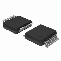
74LV165DB,112 NXP Semiconductors, 74LV165DB,112 Datasheet - Page 7

74LV165DB,112
Manufacturer Part Number
74LV165DB,112
Description
IC 8BIT SHIFT REGISTER 16SSOP
Manufacturer
NXP Semiconductors
Series
74LVr
Datasheet
1.74LV165N112.pdf
(14 pages)
Specifications of 74LV165DB,112
Logic Type
Shift Register
Output Type
Differential
Number Of Elements
1
Number Of Bits Per Element
8
Function
Parallel or Serial to Serial
Voltage - Supply
1 V ~ 5.5 V
Operating Temperature
-40°C ~ 125°C
Mounting Type
Surface Mount
Package / Case
16-SSOP
Lead Free Status / RoHS Status
Lead free / RoHS Compliant
Other names
74LV165DB
74LV165DB
935166030112
74LV165DB
935166030112
1. Unless otherwise stated, all typical values are measured at T
2. Typical values are measured at V
Philips Semiconductors
AC CHARACTERISTICS ( Continued )
GND = 0V; t
NOTES:
AC WAVEFORMS
V
V
V
output load.
Note to Figures 1 and 2
The changing to output assumes internal Q
1998 May 07
Figure 1. Clock (CP) to output (Q
SYMBOL
SYMBOL
M
M
OL
8-bit parallel-in/serial-out shift register
= 1.5 V at V
= 0.5
The changing to output assumes internal Q
the clock pulse width and the maximum clock frequency.
f
f
and V
max
t
su
t
t
h
h
CP INPUT
OUTPUT
Q
7
OH
or Q
V
GND
V
V
r
CC
OH
OL
= t
are the typical output voltage drop that occur with the
V
7
I
Set-up time
D
D
Hold time
Hold time
D
D to PL
D
Hold time
Hold time
CE to CP,
CP t CE
CP to CE
Maximum clock
pulse frequency
CC
at V
f
n
n
s
n
PARAMETER
PARAMETER
to PL
to PL
to CP, CE
to PL
2.5ns; C
CC
2.7 V.
V
M
t
PHL
2.7 V;
t
W
L
= 50pF; R
1/f
V
M
max
6
CC
7
opposite state from Q
WAVEFORM
WAVEFORM
or Q
L
Figures 1, 2
Figures 1, 2
Figures 1, 2
Figures 1 2
Figures 1, 2
= 3.3 V.
= 1K
6
opposite state from Q
7
) propagation delays,
t
PLH
7
.
SV00590
7
CONDITION
amb
.
3.0 to 3.6
4.5 to 5.5
3.0 to 3.6
4.5 to 5.5
3.0 to 3.6
4.5 to 5.5
3.0 to 3.6
4.5 to 5.5
V
CC
1.2
2.0
2.7
1.2
2.0
2.7
1.2
2.0
2.7
2.0
2.7
= 25 C
(V)
7
output (Q
Q
7
Figure 2. Parallel load (PL) pulse width, the parallel load to
The changing to output assumes internal Q
or Q
CE, CP INPUT
7
PL INPUT
OUTPUT
7
GND
GND
V
V
(CP) and clock enable (CE) removal time.
or Q
MIN
22
16
13
22
16
13
14
19
24
36
OH
OL
V
V
–
9
–
9
–
5
5
5
5
I
I
7
–40 to +85 C
) propagation delays, the parallel load to clock
TYP
–30
–5
65
25
5
20
–8
–6
–4
40
60
75
8
6
4
7
5
4
3
2
V
2
2
M
1
t
PHL
t
W
MAX
–
–
–
–
–
–
–
–
–
–
–
–
–
–
–
–
–
–
–
6
opposite state from Q
V
M
–40 to +125 C
MIN
t
rem
26
19
15
10
26
19
15
10
12
16
20
30
–
–
–
5
5
5
5
V
Product specification
M
MAX
74LV165
–
–
–
–
–
–
–
–
–
–
–
–
–
–
–
–
–
–
–
7
.
SV00591
UNIT
UNIT
MHz
MHz
ns
ns
ns


