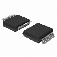
74LV165DB,112 NXP Semiconductors, 74LV165DB,112 Datasheet - Page 8

74LV165DB,112
Manufacturer Part Number
74LV165DB,112
Description
IC 8BIT SHIFT REGISTER 16SSOP
Manufacturer
NXP Semiconductors
Series
74LVr
Datasheet
1.74LV165N112.pdf
(14 pages)
Specifications of 74LV165DB,112
Logic Type
Shift Register
Output Type
Differential
Number Of Elements
1
Number Of Bits Per Element
8
Function
Parallel or Serial to Serial
Voltage - Supply
1 V ~ 5.5 V
Operating Temperature
-40°C ~ 125°C
Mounting Type
Surface Mount
Package / Case
16-SSOP
Lead Free Status / RoHS Status
Lead free / RoHS Compliant
Other names
74LV165DB
74LV165DB
935166030112
74LV165DB
935166030112
Philips Semiconductors
AC WAVEFORMS
V
V
V
output load.
Note to Figure 4
CE may change only from HIGH-to-LOW while CP is LOW. The
shaded areas indicate when the input is permitted to change for
predictable output performance.
1998 May 07
Figure 4. Set-up and hold times from the serial data input (D
enable input (CE) to the clock input (CP) and from the clock input
M
M
OL
the clock (CP) and the clock enable (CE) inputs, from the clock
8-bit parallel-in/serial-out shift register
CE may change only from HIGH-to-LOW while CP is LOW. The shaded
areas indicate when the input is permitted to change for predictable output
performance.
Figure 3. Data input (D
= 1.5 V at V
= 0.5
and V
D
S
CP, CE
CP, CE
INPUT
INPUT
INPUT
Q
Q
GND
GND
GND
OH
7
7
D
V
OUTPUT
OUTPUT
V
V
V
7
CC
I
I
I
INPUT
are the typical output voltage drop that occur with the
GND
CC
V
V
V
V
at V
OH
OH
(CP) to the clock enable input (CE).
OL
OL
V
I
CC
2.7 V.
see note
delays when PL is LOW.
V
M
t
su
2.7 V;
V
(L)
t
M
su
stable
t
t
n
V
PHL
PLH
) to output (Q
M
t
t
h
V
h
M
V
V
M
M
t
t
PHL
PLH
7
or Q
t
W
SV00592
t
su
7
) propagation
(H)
SV00595
t
h
S
) to
8
TEST CIRCUIT
Figure 5. Set-up and hold times from the data inputs (D
t
PLH/
GENERATOR
TEST
DEFINITIONS
R
C
R
D
PL INPUT
T
PULSE
L
L
t
n
PHL
= Load resistor
= Load capacitance includes jig and probe capacitiance
= Termination resistance should be equal to Z
INPUT
Figure 6. Load circuitry for switching times.
GND
GND
V
V
I
I
to the parallel load input (PL).
Test Circuit for Outputs
V
2.7–3.6V
V
l
< 2.7V
M
t
su
R
V
4.5 V
T
CC
t
V
H
M
D.U.T.
V
cc
2.7V
V
V
V
CC
CC
I
V
O
OUT
C
L
t
su
of pulse generators.
Product specification
50pF
74LV165
SV00593
t
H
SV00902
R
L
= 1k
n
)


