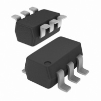
74AUP1T98GW,125 NXP Semiconductors, 74AUP1T98GW,125 Datasheet - Page 7

74AUP1T98GW,125
Manufacturer Part Number
74AUP1T98GW,125
Description
IC LP CONFIG GATE V-XLATR UMT6
Manufacturer
NXP Semiconductors
Series
74AUPr
Datasheet
1.74AUP1T98GW125.pdf
(20 pages)
Specifications of 74AUP1T98GW,125
Package / Case
SC-70-6, SC-88, SOT-363
Logic Function
Translator
Number Of Bits
3
Input Type
Voltage
Output Type
Voltage
Number Of Channels
3
Number Of Outputs/channel
1
Differential - Input:output
No/No
Propagation Delay (max)
3.8ns
Voltage - Supply
2.3 V ~ 3.6 V
Operating Temperature
-40°C ~ 125°C
Supply Voltage
2.3 V ~ 3.6 V
Logic Family
74AUP
Translation
CMOS to CMOS
Propagation Delay Time
6.8 ns
Supply Voltage (max)
3.6 V
Supply Voltage (min)
2.3 V
Maximum Operating Temperature
+ 125 C
Minimum Operating Temperature
- 40 C
Maximum Power Dissipation
250 mW
Mounting Style
SMD/SMT
Lead Free Status / RoHS Status
Lead free / RoHS Compliant
Data Rate
-
Lead Free Status / Rohs Status
Lead free / RoHS Compliant
Other names
568-4753-2
74AUP1T98GW,125
74AUP1T98GW-G
74AUP1T98GW-G
935280471125
74AUP1T98GW,125
74AUP1T98GW-G
74AUP1T98GW-G
935280471125
NXP Semiconductors
Table 8.
At recommended operating conditions; voltages are referenced to GND (ground = 0 V).
74AUP1T98
Product data sheet
Symbol Parameter
V
V
I
I
ΔI
I
ΔI
T
V
V
V
V
V
I
I
OFF
CC
I
amb
OH
OL
T+
T−
H
OH
OL
OFF
CC
= −40 °C to +125 °C
HIGH-level output voltage
LOW-level output voltage
input leakage current
power-off leakage current
additional power-off
leakage current
supply current
additional supply current
positive-going threshold
voltage
negative-going threshold
voltage
hysteresis voltage
HIGH-level output voltage
LOW-level output voltage
input leakage current
Static characteristics
…continued
Conditions
V
V
V
V
V
V
V
V
V
V
V
V
V
V
(V
V
V
V
I
I
I
I
I
CC
I
CC
CC
CC
CC
CC
CC
CC
I
I
I
I
I
I
I
I
I
I
I
I
I
H
V
V
I
I
I
I
I
I
I
I
I
I
= V
= V
= GND to 3.6 V; V
or V
or V
= GND or V
= V
= V
= GND to 3.6 V; V
O
O
O
O
O
O
O
O
O
O
O
O
O
O
O
O
O
O
O
O
All information provided in this document is subject to legal disclaimers.
CC
CC
= V
= 0 V to 0.2 V
= 2.3 V to 3.6 V
= 2.3 V to 2.7 V; I
= 3.0 V to 3.6 V; I
= 2.3 V to 2.7 V
= 3.0 V to 3.6 V
= 2.3 V to 2.7 V
= 3.0 V to 3.6 V
= −20 μA; V
= −2.3 mA; V
= −3.1 mA; V
= −2.7 mA; V
= −4.0 mA; V
= 20 μA; V
= 2.3 mA; V
= 3.1 mA; V
= 2.7 mA; V
= 4.0 mA; V
= −20 μA; V
= −2.3 mA; V
= −3.1 mA; V
= −2.7 mA; V
= −4.0 mA; V
= 20 μA; V
= 2.3 mA; V
= 3.1 mA; V
= 2.7 mA; V
= 4.0 mA; V
T+
T+
T+
T+
O
O
= 2.3 V to 2.7 V
= 3.0 V to 3.6 V
T+
or V
or V
= 0 V to 3.6 V; V
= 0 V to 3.6 V;
or V
or V
− V
Rev. 2 — 19 October 2010
T−
T−
T−
T−
T−
CC
CC
CC
)
Low-power configurable gate with voltage-level translator
CC
CC
CC
CC
CC
CC
CC
CC
CC
CC
; I
CC
CC
CC
CC
CC
CC
CC
CC
= 2.3 V to 3.6 V
= 2.3 V to 3.6 V
O
= 2.3 V to 3.6 V
= 2.3 V
= 2.3 V
= 3.0 V
= 3.0 V
= 2.3 V to 3.6 V
= 2.3 V
= 2.3 V
= 3.0 V
= 3.0 V
CC
= 0 A;
CC
= 2.3 V
= 2.3 V
= 3.0 V
= 3.0 V
= 2.3 V
= 2.3 V
= 3.0 V
= 3.0 V
O
O
= 0 V to 3.6 V
= 0 V to 3.6 V
= 0 A
= 0 A
CC
= 0 V
[1]
[2]
Min
V
-
-
-
-
-
-
-
-
-
-
V
-
-
-
-
-
1.97
1.85
2.67
2.55
-
0.60
0.75
0.33
0.46
0.10
0.15
1.77
1.67
2.40
2.30
-
CC
CC
− 0.1
− 0.11 -
Typ
-
-
-
-
-
-
-
-
-
-
-
-
-
-
-
-
-
-
-
-
-
-
-
-
-
-
-
-
-
-
-
-
74AUP1T98
© NXP B.V. 2010. All rights reserved.
Max
-
-
-
-
-
0.1
0.33
0.45
0.33
0.45
±0.5
±0.5
±0.5
1.5
4
12
1.10
1.19
0.64
0.85
0.60
0.56
-
-
-
-
-
0.11
0.36
0.50
0.36
0.50
±0.75
7 of 20
V
V
V
V
V
V
V
V
Unit
V
V
V
V
V
V
μA
μA
μA
μA
μA
μA
V
V
V
V
V
V
V
V
V
V
V
V
μA


