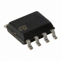
M24M01-RMN6TP STMicroelectronics, M24M01-RMN6TP Datasheet - Page 15

M24M01-RMN6TP
Manufacturer Part Number
M24M01-RMN6TP
Description
IC EEPROM 1MBIT 400KHZ 8SOIC
Manufacturer
STMicroelectronics
Datasheet
1.M24M01-RMW6TG.pdf
(37 pages)
Specifications of M24M01-RMN6TP
Format - Memory
EEPROMs - Serial
Memory Type
EEPROM
Memory Size
1M (128K x 8)
Speed
400kHz
Interface
I²C, 2-Wire Serial
Voltage - Supply
1.8 V ~ 5.5 V
Operating Temperature
-40°C ~ 85°C
Package / Case
8-SOIC (3.9mm Width)
Organization
128 K x 8
Interface Type
I2C
Maximum Clock Frequency
0.4 MHz
Access Time
900 ns
Supply Voltage (max)
5.5 V
Supply Voltage (min)
1.8 V
Maximum Operating Current
2 mA
Maximum Operating Temperature
+ 85 C
Mounting Style
SMD/SMT
Minimum Operating Temperature
- 40 C
Operating Supply Voltage
2.5 V, 3.3 V, 5 V
Lead Free Status / RoHS Status
Lead free / RoHS Compliant
Other names
497-6351-2
Available stocks
Company
Part Number
Manufacturer
Quantity
Price
Part Number:
M24M01-RMN6TP
Manufacturer:
ST
Quantity:
20 000
M24M01-R, M24M01-W, M24M01-HR
3.6
3.7
3.8
Write operations
Following a Start condition the bus master sends a device select code with the R/W bit (RW)
reset to 0. The device acknowledges this, as shown in
bytes. The device responds to each address byte with an acknowledge bit, and then waits
for the data byte.
Writing to the memory may be inhibited if Write Control (WC) is driven high. Any Write
instruction with Write Control (WC) driven high (during a period of time from the Start
condition until the end of the two address bytes) will not modify the memory contents, and
the accompanying data bytes are not acknowledged, as shown in
Each data byte in the memory has a 17-bit address (the most significant bit b16 is in the
device select code and the Least Significant Bits b15-b0 are defined in two address bytes).
The most significant byte
(Table
When the bus master generates a Stop condition immediately after the Ack bit (in the “10
bit” time slot), either at the end of a Byte Write or a Page Write, the internal memory Write
cycle is triggered. A Stop condition at any other time slot does not trigger the internal Write
cycle.
After the Stop condition, the delay t
the device’s internal address counter is incremented automatically, to point to the next byte
address after the last one that was modified.
During the internal Write cycle, Serial Data (SDA) is disabled internally, and the device does
not respond to any requests.
Byte Write
After the device select code and the address bytes, the bus master sends one data byte. If
the addressed location is Write-protected, by Write Control (WC) being driven high, the
device replies with NoAck, and the location is not modified. If, instead, the addressed
location is not Write-protected, the device replies with Ack. The bus master terminates the
transfer by generating a Stop condition, as shown in
Page Write
The Page Write mode allows up to 256 bytes to be written in a single Write cycle, provided
that they are all located in the same ’row’ in the memory: that is, the most significant
memory address bits, b16-b8, are the same. If more bytes are sent than will fit up to the end
of the row, a condition known as ‘roll-over’ occurs. This should be avoided, as data starts to
become overwritten in an implementation dependent way.
The bus master sends from 1 to 256 bytes of data, each of which is acknowledged by the
device if Write Control (WC) is low. If Write Control (WC) is high, the contents of the
addressed memory location are not modified, and each data byte is followed by a NoAck.
After each byte is transferred, the internal byte address counter (the 8 least significant
address bits only) is incremented. The transfer is terminated by the bus master generating a
Stop condition.
4).
(Table
Doc ID 12943 Rev 7
3) is sent first, followed by the least significant byte
W
, and the successful completion of a Write operation,
Figure
Figure
9.
9, and waits for two address
Figure
8.
Device operation
15/37
th


