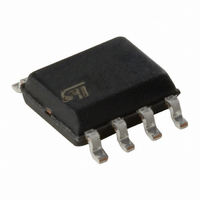
M24M01-RMN6TP STMicroelectronics, M24M01-RMN6TP Datasheet - Page 19

M24M01-RMN6TP
Manufacturer Part Number
M24M01-RMN6TP
Description
IC EEPROM 1MBIT 400KHZ 8SOIC
Manufacturer
STMicroelectronics
Datasheet
1.M24M01-RMW6TG.pdf
(37 pages)
Specifications of M24M01-RMN6TP
Format - Memory
EEPROMs - Serial
Memory Type
EEPROM
Memory Size
1M (128K x 8)
Speed
400kHz
Interface
I²C, 2-Wire Serial
Voltage - Supply
1.8 V ~ 5.5 V
Operating Temperature
-40°C ~ 85°C
Package / Case
8-SOIC (3.9mm Width)
Organization
128 K x 8
Interface Type
I2C
Maximum Clock Frequency
0.4 MHz
Access Time
900 ns
Supply Voltage (max)
5.5 V
Supply Voltage (min)
1.8 V
Maximum Operating Current
2 mA
Maximum Operating Temperature
+ 85 C
Mounting Style
SMD/SMT
Minimum Operating Temperature
- 40 C
Operating Supply Voltage
2.5 V, 3.3 V, 5 V
Lead Free Status / RoHS Status
Lead free / RoHS Compliant
Other names
497-6351-2
Available stocks
Company
Part Number
Manufacturer
Quantity
Price
Part Number:
M24M01-RMN6TP
Manufacturer:
ST
Quantity:
20 000
M24M01-R, M24M01-W, M24M01-HR
3.11
3.12
3.13
3.14
3.15
Read operations
Read operations are performed independently of the state of the Write Control (WC) signal.
After the successful completion of a Read operation, the device’s internal address counter is
incremented by one, to point to the next byte address.
Random Address Read
A dummy Write is first performed to load the address into this address counter (as shown in
Figure
condition, and repeats the device select code, with the RW bit set to 1. The device
acknowledges this, and outputs the contents of the addressed byte. The bus master must
not acknowledge the byte, and terminates the transfer with a Stop condition.
Current Address Read
For the Current Address Read operation, following a Start condition, the bus master only
sends a device select code with the R/W bit set to 1. The device acknowledges this, and
outputs the byte addressed by the internal address counter. The counter is then
incremented. The bus master terminates the transfer with a Stop condition, as shown in
Figure
Sequential Read
This operation can be used after a Current Address Read or a Random Address Read. The
bus master does acknowledge the data byte output, and sends additional clock pulses so
that the device continues to output the next byte in sequence. To terminate the stream of
bytes, the bus master must not acknowledge the last byte, and must generate a Stop
condition, as shown in
The output data comes from consecutive addresses, with the internal address counter
automatically incremented after each byte output. After the last memory address, the
address counter ‘rolls-over’, and the device continues to output data from memory address
00h.
Acknowledge in Read mode
For all Read instructions, the device waits, after each byte read, for an acknowledgment
during the 9
time, the device terminates the data transfer and switches to its Standby mode.
11) but without sending a Stop condition. Then, the bus master sends another Start
11, without acknowledging the byte.
th
bit time. If the bus master does not drive Serial Data (SDA) low during this
Figure
11.
Doc ID 12943 Rev 7
Device operation
19/37


