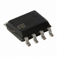
M24M01-RMN6TP STMicroelectronics, M24M01-RMN6TP Datasheet - Page 18

M24M01-RMN6TP
Manufacturer Part Number
M24M01-RMN6TP
Description
IC EEPROM 1MBIT 400KHZ 8SOIC
Manufacturer
STMicroelectronics
Datasheet
1.M24M01-RMW6TG.pdf
(37 pages)
Specifications of M24M01-RMN6TP
Format - Memory
EEPROMs - Serial
Memory Type
EEPROM
Memory Size
1M (128K x 8)
Speed
400kHz
Interface
I²C, 2-Wire Serial
Voltage - Supply
1.8 V ~ 5.5 V
Operating Temperature
-40°C ~ 85°C
Package / Case
8-SOIC (3.9mm Width)
Organization
128 K x 8
Interface Type
I2C
Maximum Clock Frequency
0.4 MHz
Access Time
900 ns
Supply Voltage (max)
5.5 V
Supply Voltage (min)
1.8 V
Maximum Operating Current
2 mA
Maximum Operating Temperature
+ 85 C
Mounting Style
SMD/SMT
Minimum Operating Temperature
- 40 C
Operating Supply Voltage
2.5 V, 3.3 V, 5 V
Lead Free Status / RoHS Status
Lead free / RoHS Compliant
Other names
497-6351-2
Available stocks
Company
Part Number
Manufacturer
Quantity
Price
Part Number:
M24M01-RMN6TP
Manufacturer:
ST
Quantity:
20 000
Device operation
3.10
18/37
Minimizing system delays by polling on ACK
During the internal Write cycle, the device disconnects itself from the bus, and writes a copy
of the data from its internal latches to the memory cells. The maximum Write time (t
shown in
can be used by the bus master.
The sequence, as shown in
●
●
●
Figure 11. Read mode sequences
1. The seven most significant bits of the device select code of a Random Read (in the 1
Current
Address
Read
Random
Address
Read
Sequential
Current
Read
Sequention
Random
Read
be identical.
Initial condition: a Write cycle is in progress.
Step 1: the bus master issues a Start condition followed by a device select code (the
first byte of the new instruction).
Step 2: if the device is busy with the internal Write cycle, no Ack will be returned and
the bus master goes back to Step 1. If the device has terminated the internal Write
cycle, it responds with an Ack, indicating that the device is ready to receive the second
part of the instruction (the first byte of this instruction having been sent during Step 1).
Table
13, but the typical time is shorter. To make use of this, a polling sequence
Dev sel *
Dev sel *
ACK
Dev sel
Dev sel
Data out N
Figure
R/W
R/W
R/W
Doc ID 12943 Rev 7
ACK
ACK
ACK
ACK
R/W
NO ACK
10, is:
Data out 1
Byte addr
Byte addr
Data out
NO ACK
ACK
ACK
ACK
Byte addr
Byte addr
M24M01-R, M24M01-W, M24M01-HR
ACK
ACK
ACK
Data out N
Dev sel *
Dev sel *
NO ACK
R/W
st
ACK
ACK
R/W
and 4
Data out1
Data out
th
bytes) must
NO ACK
AI01105d
w
ACK
) is


