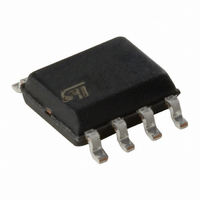
M24M01-RMN6TP STMicroelectronics, M24M01-RMN6TP Datasheet - Page 25

M24M01-RMN6TP
Manufacturer Part Number
M24M01-RMN6TP
Description
IC EEPROM 1MBIT 400KHZ 8SOIC
Manufacturer
STMicroelectronics
Datasheet
1.M24M01-RMW6TG.pdf
(37 pages)
Specifications of M24M01-RMN6TP
Format - Memory
EEPROMs - Serial
Memory Type
EEPROM
Memory Size
1M (128K x 8)
Speed
400kHz
Interface
I²C, 2-Wire Serial
Voltage - Supply
1.8 V ~ 5.5 V
Operating Temperature
-40°C ~ 85°C
Package / Case
8-SOIC (3.9mm Width)
Organization
128 K x 8
Interface Type
I2C
Maximum Clock Frequency
0.4 MHz
Access Time
900 ns
Supply Voltage (max)
5.5 V
Supply Voltage (min)
1.8 V
Maximum Operating Current
2 mA
Maximum Operating Temperature
+ 85 C
Mounting Style
SMD/SMT
Minimum Operating Temperature
- 40 C
Operating Supply Voltage
2.5 V, 3.3 V, 5 V
Lead Free Status / RoHS Status
Lead free / RoHS Compliant
Other names
497-6351-2
Available stocks
Company
Part Number
Manufacturer
Quantity
Price
Part Number:
M24M01-RMN6TP
Manufacturer:
ST
Quantity:
20 000
M24M01-R, M24M01-W, M24M01-HR
Table 14.
1. Input rise/fall time values recommended by the Fast-mode Plus I²C-bus specification. The M24xxx devices
2. Characterized only, not tested in production.
3. The SDA(out) rise time is not defined by the M24xxx, it is defined by the application pull-up resistor
4. To avoid spurious Start and Stop conditions, a minimum delay is placed between SCL=1 and the falling or
5. t
6. For a reStart condition, or following a Write cycle.
f
t
t
t
t
t
t
t
t
t
t
t
t
t
t
t
C
CHCL
CLCH
XH1XH2
XL1XL2
QL1QL2
DXCH
CLDX
CLQX
CLQV
CHDL
DLCL
CHDH
DHDL
W
NS
Symbol
accept longer input rise/fall times provided that these rise/fall times are compatible with all other timing
conditions defined in this AC table.
(connected on the SDA line) and, therefore, it is not specified in this table.
rising edge of SDA.
that the R
(2)
CLQV
(4)(5)
(6)
(1)
(2)(3)
(1)
is the time (from the falling edge of SCL) required by the SDA bus line to reach 0.8V
bus
AC characteristics at 1 MHz (M24M01-HR)
f
t
t
t
t
t
t
t
t
t
t
t
t
SCL
HIGH
LOW
R
F
F
SU:DAT
SU:STA
HD:STA
SU:STO
BUF
WR
× C
HD:DAT
Alt.
t
t
DH
AA
bus
time constant is within the range defined in
Clock frequency
Clock pulse width high
Clock pulse width low
Input signal rise time
Input signal fall time
SDA (out) fall time
Data in setup time
Data in hold time
Data out hold time
Clock low to next data valid (access time)
Start condition setup time
Start condition hold time
Stop condition setup time
Time between Stop condition and next
Start condition
Write time
Pulse width ignored (input filter on SCL
and SDA)
Test conditions specified in
Doc ID 12943 Rev 7
Parameter
Figure
Table 7
6.
0
300
400
-
-
-
80
0
50
50
250
250
250
500
-
-
Min.
DC and AC parameters
1
-
-
120
120
120
-
-
-
500
-
-
-
-
5
50
Max.
CC
, assuming
MHz
ns
ns
ns
ns
ns
ns
ns
ns
ns
ns
ns
ns
ns
ms
ns
Unit
25/37


