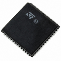
PSD813F2A-90J STMicroelectronics, PSD813F2A-90J Datasheet - Page 13

PSD813F2A-90J
Manufacturer Part Number
PSD813F2A-90J
Description
IC FLASH 1MBIT 90NS 52PLCC
Manufacturer
STMicroelectronics
Datasheet
1.PSD813F2VA-20JI.pdf
(109 pages)
Specifications of PSD813F2A-90J
Format - Memory
FLASH
Memory Type
FLASH
Memory Size
1M (128K x 8)
Speed
90ns
Interface
Parallel
Voltage - Supply
4.5 V ~ 5.5 V
Operating Temperature
0°C ~ 70°C
Package / Case
52-PLCC
Lead Free Status / RoHS Status
Lead free / RoHS Compliant
Other names
497-1988-5
Available stocks
Company
Part Number
Manufacturer
Quantity
Price
Company:
Part Number:
PSD813F2A-90J
Manufacturer:
ST
Quantity:
6
Company:
Part Number:
PSD813F2A-90J
Manufacturer:
STMicroelectronics
Quantity:
10 000
Company:
Part Number:
PSD813F2A-90JI
Manufacturer:
FSC
Quantity:
30 000
Company:
Part Number:
PSD813F2A-90JI
Manufacturer:
STMicroelectronics
Quantity:
10 000
Part Number:
PSD813F2A-90JI
Manufacturer:
ST
Quantity:
20 000
Note: 1. The pin numbers in this table are for the PLCC package only. See the package information from
Pin Name
GND
PC7
PD0
PD1
PD2
V
2. These functions can be multiplexed with other functions.
CC
77., page 107
15, 38
1, 16,
Pin
11
10
26
9
8
for pin numbers on other package types.
Type
I/O
I/O
I/O
I/O
PC7 pin of Port C. This port pin can be configured to have the following functions:
MCU I/O – write to or read from a standard output or input port.
CPLD macrocell (McellBC7) output.
Input to the PLDs.
DBE – active Low Data Byte Enable input from 68HC912 type MCUs.
This pin can be configured as a CMOS or Open Drain output.
PD0 pin of Port D. This port pin can be configured to have the following functions:
ALE/AS input latches address output from the MCU.
MCU I/O – write or read from a standard output or input port.
Input to the PLDs.
CPLD output (External Chip Select).
PD1 pin of Port D. This port pin can be configured to have the following functions:
MCU I/O – write to or read from a standard output or input port.
Input to the PLDs.
CPLD output (External Chip Select).
CLKIN – clock input to the CPLD macrocells, the APD Unit’s Power-down counter, and
the CPLD AND Array.
PD2 pin of Port D. This port pin can be configured to have the following functions:
MCU I/O - write to or read from a standard output or input port.
Input to the PLDs.
CPLD output (External Chip Select).
PSD Chip Select Input (CSI). When Low, the MCU can access the PSD memory and I/O.
When High, the PSD memory blocks are disabled to conserve power.
Supply Voltage
Ground pins
Doc ID 10552 Rev 3
Description
PSD813F2V, PSD854F2V
Table 75., page 105
and
13/109
Table


