PSD813F2A-90J STMicroelectronics, PSD813F2A-90J Datasheet - Page 27
PSD813F2A-90J
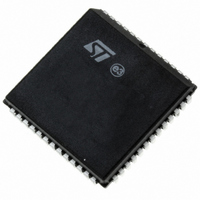
Manufacturer Part Number
PSD813F2A-90J
Description
IC FLASH 1MBIT 90NS 52PLCC
Manufacturer
STMicroelectronics
Datasheet
1.PSD813F2VA-20JI.pdf
(109 pages)
Specifications of PSD813F2A-90J
Format - Memory
FLASH
Memory Type
FLASH
Memory Size
1M (128K x 8)
Speed
90ns
Interface
Parallel
Voltage - Supply
4.5 V ~ 5.5 V
Operating Temperature
0°C ~ 70°C
Package / Case
52-PLCC
Lead Free Status / RoHS Status
Lead free / RoHS Compliant
Other names
497-1988-5
Available stocks
Company
Part Number
Manufacturer
Quantity
Price
Company:

Part Number:
PSD813F2A-90J
Manufacturer:
ST
Quantity:
6
Company:
Part Number:
PSD813F2A-90J
Manufacturer:
STMicroelectronics
Quantity:
10 000
Company:
Part Number:
PSD813F2A-90JI
Manufacturer:
FSC
Quantity:
30 000
Company:
Part Number:
PSD813F2A-90JI
Manufacturer:
STMicroelectronics
Quantity:
10 000
Part Number:
PSD813F2A-90JI
Manufacturer:
ST
Quantity:
20 000


ERASING FLASH MEMORY
Flash Bulk Erase
The Flash Bulk Erase instruction uses six WRITE
operations followed by a READ operation of the
status register, as described in
If any byte of the Bulk Erase instruction is wrong,
the Bulk Erase instruction aborts and the device is
reset to the Read Flash memory status.
During a Bulk Erase, the memory status may be
checked by reading the Error Flag Bit (DQ5), the
Toggle Flag Bit (DQ6), and the Data Polling Flag
Bit (DQ7), as detailed in the section entitled
GRAMMING FLASH MEMORY, page
ror Flag Bit (DQ5) returns a '1' if there has been an
Erase Failure (maximum number of Erase cycles
have been executed).
It is not necessary to program the memory with
00h because the PSD automatically does this be-
fore erasing to 0FFh.
During execution of the Bulk Erase instruction, the
Flash memory does not accept any instructions.
Flash Sector Erase
The Sector Erase instruction uses six WRITE op-
erations, as described in
tional Flash Sector Erase codes and Flash
memory sector addresses can be written subse-
quently to erase other Flash memory sectors in
parallel, without further coded cycles, if the addi-
tional bytes are transmitted in a shorter time than
the time-out period of about 100µs. The input of a
new Sector Erase code restarts the time-out peri-
od.
The status of the internal timer can be monitored
through the level of the Erase Time-out Flag Bit
(DQ3). If the Erase Time-out Flag Bit (DQ3) is ’0,’
the Sector Erase instruction has been received
and the time-out period is counting. If the Erase
Time-out Flag Bit (DQ3) is '1,' the time-out period
has expired and the PSD is busy erasing the Flash
memory sector(s). Before and during Erase time-
out, any instruction other than Suspend Sector
Erase and Resume Sector Erase instructions
abort the cycle that is currently in progress, and re-
set the device to READ Mode. It is not necessary
to program the Flash memory sector with 00h as
the PSD does this automatically before erasing
(byte = FFh).
During a Sector Erase, the memory status may be
checked by reading the Error Flag Bit (DQ5), the
Toggle Flag Bit (DQ6), and the Data Polling Flag
Bit (DQ7), as detailed in the section entitled
GRAMMING FLASH MEMORY, page
Table 9., page
Table 9., page
25. The Er-
25.
Doc ID 10552 Rev 3
21. Addi-
PRO-
PRO-
21.
During execution of the Erase cycle, the Flash
memory accepts only Reset and Suspend Sector
Erase instructions. Erasure of one Flash memory
sector may be suspended, in order to read data
from another Flash memory sector, and then re-
sumed.
Suspend Sector Erase
When a Sector Erase cycle is in progress, the Sus-
pend Sector Erase instruction can be used to sus-
pend the cycle by writing 0B0h to any address
when an appropriate Sector Select (FS0-FS7 or
CSBOOT0-CSBOOT3) is High. (See
9., page
other Flash memory sector after the Erase cycle
has been suspended. Suspend Sector Erase is
accepted only during an Erase cycle and defaults
to READ Mode. A Suspend Sector Erase instruc-
tion executed during an Erase time-out period, in
addition to suspending the Erase cycle, terminates
the time out period.
The Toggle Flag Bit (DQ6) stops toggling when the
PSD internal logic is suspended. The status of this
bit must be monitored at an address within the
Flash memory sector being erased. The Toggle
Flag Bit (DQ6) stops toggling between 0.1µs and
15µs after the Suspend Sector Erase instruction
has been executed. The PSD is then automatically
set to READ Mode.
If an Suspend Sector Erase instruction was exe-
cuted, the following rules apply:
–
–
–
–
Resume Sector Erase
If a Suspend Sector Erase instruction was previ-
ously executed, the erase cycle may be resumed
with this instruction. The Resume Sector Erase in-
struction consists of writing 030h to any address
while an appropriate Sector Select (FS0-FS7 or
CSBOOT0-CSBOOT3) is High. (See
9., page
Attempting to read from a Flash memory
sector that was being erased outputs invalid
data.
Reading from a Flash sector that was not
being erased is valid.
The Flash memory cannot be programmed,
and only responds to Resume Sector Erase
and Reset Flash instructions (READ is an
operation and is allowed).
If a Reset Flash instruction is received, data in
the Flash memory sector that was being
erased is invalid.
21). This allows reading of data from an-
21.)
PSD813F2V, PSD854F2V
27/109
Table
Table
Related parts for PSD813F2A-90J
Image
Part Number
Description
Manufacturer
Datasheet
Request
R

Part Number:
Description:
Manufacturer:
STMicroelectronics
Datasheet:
Part Number:
Description:
Flash In-System-Programmable Microcontroller Peripheral
Manufacturer:
STMicroelectronics
Part Number:
Description:
Manufacturer:
STMicroelectronics
Datasheet:
Part Number:
Description:
STMicroelectronics [RIPPLE-CARRY BINARY COUNTER/DIVIDERS]
Manufacturer:
STMicroelectronics
Datasheet:
Part Number:
Description:
STMicroelectronics [LIQUID-CRYSTAL DISPLAY DRIVERS]
Manufacturer:
STMicroelectronics
Datasheet:

Part Number:
Description:
BOARD EVAL FOR MEMS SENSORS
Manufacturer:
STMicroelectronics
Datasheet:
Part Number:
Description:
NPN TRANSISTOR POWER MODULE
Manufacturer:
STMicroelectronics
Datasheet:
Part Number:
Description:
TURBOSWITCH ULTRA-FAST HIGH VOLTAGE DIODE
Manufacturer:
STMicroelectronics
Datasheet:
Part Number:
Description:
Manufacturer:
STMicroelectronics
Datasheet:
Part Number:
Description:
DIODE / SCR MODULE
Manufacturer:
STMicroelectronics
Datasheet:
Part Number:
Description:
DIODE / SCR MODULE
Manufacturer:
STMicroelectronics
Datasheet:
Part Number:
Description:
Search -----> STE16N100
Manufacturer:
STMicroelectronics
Datasheet: