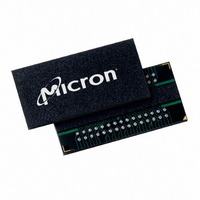
MT41J128M8HX-187E:D TR Micron Technology Inc, MT41J128M8HX-187E:D TR Datasheet - Page 102

MT41J128M8HX-187E:D TR
Manufacturer Part Number
MT41J128M8HX-187E:D TR
Description
IC DDR3 SDRAM 1GBIT 78FBGA
Manufacturer
Micron Technology Inc
Datasheet
1.MT41J64M16LA-187EB_TR.pdf
(181 pages)
Specifications of MT41J128M8HX-187E:D TR
Format - Memory
RAM
Memory Type
DDR3 SDRAM
Memory Size
1G (128M x 8)
Speed
533MHz
Interface
Parallel
Voltage - Supply
1.425 V ~ 1.575 V
Operating Temperature
0°C ~ 95°C
Package / Case
78-FBGA
Lead Free Status / RoHS Status
Lead free / RoHS Compliant
Other names
557-1377-1
- Current page: 102 of 181
- Download datasheet (9Mb)
Table 67:
PDF: 09005aef826aa906/Source: 09005aef82a357c3
1Gb_DDR3_4.fm - Rev. F 11/08 EN
Leveling
Disabled
Enabled
MR1[7]
Write
(1)
MR1[12]
Disabled
Enabled
Write Leveling Matrix
Note 1 applies to the entire table
Output
Buffers
(1)
(0)
Notes:
MR1[3, 6, 9]
40Ω, 60Ω, or
40Ω, 60Ω, or
20Ω, 30Ω,
See normal operations
R
When write leveling is enabled, the rising edge of DQS samples CK, and the prime DQ
outputs the sampled CK’s status. The prime DQ for a x4 or x8 configuration is DQ0 with
all other DQ (DQ[7:1]) driving LOW. The prime DQ for a x16 configuration is DQ0 for the
lower byte and DQ8 for the upper byte. It outputs the status of CK sampled by LDQS and
UDQS. All other DQ (DQ[7:1], DQ[15:9]) continue to drive LOW. Two prime DQ on a x16
enable each byte lane to be leveled independently.
The write leveling mode register interacts with other mode registers to correctly
configure the write leveling functionality. Besides using MR1[7] to disable/enable write
leveling, MR1[12] must be used to enable/disable the output buffers. The ODT value,
burst length, and so forth need to be selected as well. This interaction is shown in
Table 67. It should also be noted that when the outputs are enabled during write leveling
mode, the DQS buffers are set as inputs, and the DQ are set as outputs. Additionally,
during write leveling mode, only the DQS strobe terminations are activated and deacti-
vated via the ODT ball. The DQ remain disabled and are not affected by the ODT ball
(see Table 67).
Value
1. Expected usage if used during write leveling: Case 1 may be used when DRAM are on a
2. Since the DRAM DQS is not being driven (MR1[12] = 1), DQS ignores the input strobe, and
3. Since the DRAM DQS is being driven (MR1[12] = 0), DQS captures the input strobe, and only
TT
120Ω
120Ω
n/a
n/a
_
NOM
dual-rank module and on the rank not being levelized or on any rank of a module not
being levelized on a multislotted system. Case 2 may be used when DRAM are on any rank
of a module not being levelized on a multislotted system. Case 3 is generally not used. Case
4 is generally used when DRAM are on the rank that is being leveled.
all R
some R
TT
_
TT
NOM
ODT Ball
_
DRAM
NOM
High
High
Low
Low
values are allowed. This simulates a normal standby state to DQS.
values are allowed. This simulates a normal write state to DQS.
DQS
Off
Off
On
On
R
DRAM
TT
_
NOM
DQ
Off
102
Prime DQ driving CK state: not terminated
Prime DQ driving CK state: not terminated
Other DQ driving LOW: not terminated
Other DQ driving LOW: not terminated
DQS not receiving: terminated by R
DQS not receiving: not terminated
Prime DQ High-Z: not terminated
Other DQ High-Z: not terminated
Prime DQ High-Z: not terminated
Other DQ High-Z: not terminated
DQS receiving: terminated by R
Micron Technology, Inc., reserves the right to change products or specifications without notice.
DQS receiving: not terminated
Write leveling not enabled
DRAM State
1Gb: x4, x8, x16 DDR3 SDRAM
©2006 Micron Technology, Inc. All rights reserved.
TT
TT
Commands
Case Notes
0
1
2
3
4
2
3
Related parts for MT41J128M8HX-187E:D TR
Image
Part Number
Description
Manufacturer
Datasheet
Request
R

Part Number:
Description:
IC DDR3 SDRAM 1GBIT 78FBGA
Manufacturer:
Micron Technology Inc
Datasheet:

Part Number:
Description:
Manufacturer:
Micron Technology Inc
Datasheet:

Part Number:
Description:
1Gb: x4, x8, x16 DDR3 SDRAM
Manufacturer:
MDTIC [Micon Design Technology Corporation]
Datasheet:

Part Number:
Description:
IC SDRAM 64MBIT 133MHZ 54TSOP
Manufacturer:
Micron Technology Inc
Datasheet:

Part Number:
Description:
IC SDRAM 64MBIT 5.5NS 86TSOP
Manufacturer:
Micron Technology Inc
Datasheet:

Part Number:
Description:
IC SDRAM 64MBIT 200MHZ 86TSOP
Manufacturer:
Micron Technology Inc
Datasheet:

Part Number:
Description:
IC SDRAM 64MBIT 133MHZ 54TSOP
Manufacturer:
Micron Technology Inc
Datasheet:

Part Number:
Description:
IC SDRAM 128MBIT 133MHZ 54TSOP
Manufacturer:
Micron Technology Inc
Datasheet:

Part Number:
Description:
IC SDRAM 256MBIT 133MHZ 90VFBGA
Manufacturer:
Micron Technology Inc
Datasheet:

Part Number:
Description:
IC SDRAM 128MBIT 133MHZ 54TSOP
Manufacturer:
Micron Technology Inc
Datasheet:

Part Number:
Description:
IC SDRAM 256MBIT 133MHZ 54TSOP
Manufacturer:
Micron Technology Inc
Datasheet:

Part Number:
Description:
IC DDR SDRAM 512MBIT 6NS 66TSOP
Manufacturer:
Micron Technology Inc
Datasheet:

Part Number:
Description:
IC SDRAM 128MBIT 167MHZ 86TSOP
Manufacturer:
Micron Technology Inc
Datasheet:

Part Number:
Description:
IC SDRAM 128MBIT 143MHZ 86TSOP
Manufacturer:
Micron Technology Inc
Datasheet:

Part Number:
Description:
SDRAM 256M-BIT 1.8V 54-PIN VFBGA
Manufacturer:
Micron Technology Inc
Datasheet:


