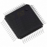
DSM2190F4V-15T6 STMicroelectronics, DSM2190F4V-15T6 Datasheet - Page 10

DSM2190F4V-15T6
Manufacturer Part Number
DSM2190F4V-15T6
Description
IC FLASH 2MBIT 150NS 52QFP
Manufacturer
STMicroelectronics
Datasheet
1.DSM2190F4V-15K6.pdf
(61 pages)
Specifications of DSM2190F4V-15T6
Format - Memory
FLASH
Memory Type
FLASH
Memory Size
2M (256K x 8)
Speed
150ns
Interface
Parallel
Voltage - Supply
3 V ~ 3.6 V
Operating Temperature
-40°C ~ 85°C
Package / Case
52-QFP
Operating Supply Voltage (typ)
3.3V
Operating Supply Voltage (min)
3V
Operating Supply Voltage (max)
3.6V
Operating Temp Range
-40C to 85C
Operating Temperature Classification
Industrial
Mounting
Surface Mount
Pin Count
52
Lead Free Status / RoHS Status
Lead free / RoHS Compliant
Other names
497-1323
Available stocks
Company
Part Number
Manufacturer
Quantity
Price
Company:
Part Number:
DSM2190F4V-15T6
Manufacturer:
STMicroelectronics
Quantity:
10 000
DSM2190F4
TYPICAL CONNECTIONS
Figure 6 shows a typical connection scheme.
Many connection possibilities exist since many
DSM pins are multipurpose. This scheme illus-
trates the use of a combined function
(functions as
also illustrates how to chain the DSM and DSP de-
vices together on the JTAG bus. The JTAG con-
nector definition depends on development and
production environment requirements. A specially
defined connector can be devised to combine the
signals of the FlashLINK and the Analog Devices
emulator. Alternatively, two separate JTAG con-
nectors can be used, one matching the pinout of
FlashLINK and the other matching the emulator pi-
nout.
Keep in mind that signals
ADDR16, ADDR17, ADDR18 can be connected to
any DSM pin that is a PLD input. I/O pins on Port
B and Port C are more capable (more PLD func-
tions) than Port D pins. It is recommended to use
Port D pins primarily for decode inputs first, leav-
ing pins on Port B and Port C available for general
10/61
BMS
and
MSx
), and many I/O pins. It
BMS
,
IOMS
BSM
,
signal
MSx
,
logic. Figure 6 illustrates a common way to make
connections.
Following are connection options to consider:
Port C JTAG: Figure 6 shows four JTAG signals
(TMS, TCK, TDI, TDO) connected to the DSM. Al-
ternatively, using six-pin JTAG (two more signals,
TSTAT and
much as 30% compared to four-pin JTAG. Other
JTAG options include multiplexing JTAG pins with
general I/O (see “Programming In-Circuit using
JTAG ISP” on page 40 and Application Note
AN1153 ), or not using JTAG at all. If no JTAG is
used, the DSM device has to be programmed on a
conventional programmer before it is installed on
the circuit board. Using no JTAG makes more
DSM I/O available.
Pins PC2 and PD2. If not all 288K address loca-
tions need to be decoded in the DSM, then
ADDR18 on pin PD2 is not needed. In this case,
the
ing pin PC2 for general I/O usage.
IOMS
signal can be connected to pin PD2, free-
TERR
) can reduce ISP time by as


