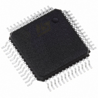
DSM2190F4V-15T6 STMicroelectronics, DSM2190F4V-15T6 Datasheet - Page 21

DSM2190F4V-15T6
Manufacturer Part Number
DSM2190F4V-15T6
Description
IC FLASH 2MBIT 150NS 52QFP
Manufacturer
STMicroelectronics
Datasheet
1.DSM2190F4V-15K6.pdf
(61 pages)
Specifications of DSM2190F4V-15T6
Format - Memory
FLASH
Memory Type
FLASH
Memory Size
2M (256K x 8)
Speed
150ns
Interface
Parallel
Voltage - Supply
3 V ~ 3.6 V
Operating Temperature
-40°C ~ 85°C
Package / Case
52-QFP
Operating Supply Voltage (typ)
3.3V
Operating Supply Voltage (min)
3V
Operating Supply Voltage (max)
3.6V
Operating Temp Range
-40C to 85C
Operating Temperature Classification
Industrial
Mounting
Surface Mount
Pin Count
52
Lead Free Status / RoHS Status
Lead free / RoHS Compliant
Other names
497-1323
Available stocks
Company
Part Number
Manufacturer
Quantity
Price
Company:
Part Number:
DSM2190F4V-15T6
Manufacturer:
STMicroelectronics
Quantity:
10 000
Figure 11. Data Toggle Flowchart
The Error Flag (DQ5) bit is set if either an internal
time-out occurred while the embedded algorithm
attempted to program the byte, or if the DSP at-
tempted to program a 1 to a bit that was not erased
(not erased is logic 0).
It is suggested (as with all Flash memories) to read
the location again after the embedded program-
ming algorithm has completed, to compare the
byte that was written to Flash memory with the
byte that was intended to be written.
When using the Data Toggle method after an
Erase cycle, Figure 11 still applies. the Toggle
Flag (DQ6) bit toggles until the Erase cycle is com-
plete. A 1 on the Error Flag (DQ5) bit indicates a
time-out condition on the Erase cycle, a 0 indi-
cates no error. The DSP can read any location
within the sector being erased to get the Toggle
Flag (DQ6) bit and the Error Flag (DQ5) bit.
PSDsoft Express generates ANSI C code func-
tions which implement these Data Toggling algo-
rithms.
Erasing Flash Memory
Flash Bulk Erase. The Flash Bulk Erase instruc-
tion sequence uses six write operations followed
by a read operation of the status register, as de-
scribed in Table 5. If any byte of the Bulk Erase in-
struction sequence is wrong, the Bulk Erase
instruction sequence aborts and the device is re-
NO
DQ5 & DQ6
READ DQ6
TOGGLE
TOGGLE
START
READ
DQ6
DQ5
DQ6
FAIL
= 1
=
=
YES
YES
YES
NO
NO
PASS
AI01370B
set to the Read Flash memory status. The Bulk
Erase command may be addresses to any one in-
dividual valid Flash memory segment ( FS0-FS7 or
CSBOOT0-CSBOOT3 ) and the entire array (all
segments in one array) will be erased.
During a Bulk Erase, the memory status may be
checked by reading the Error Flag (DQ5) bit, the
Toggle Flag (DQ6) bit, and the Data Polling Flag
(DQ7) bit, as detailed in the section entitled “Pro-
gramming Flash Memory”, on page 19. The Error
Flag (DQ5) bit returns a 1 if there has been an
Erase Failure (maximum number of Erase cycles
have been executed).
It is not necessary to program the memory with
00h because the device automatically does this
before erasing to 0FFh.
During execution of the Bulk Erase instruction se-
quence, the Flash memory does not accept any in-
struction sequences.
The address provided with the Flash Bulk Erase
command sequence (Table 5) may select any one
of the eight internal Flash memory Sector Select
signals FS0 - FS7 or one of the four signals
CSBOOT0-CSBOOT3. An erase of that entire
Flash memory array will occur even though the
command was sent to just one Flash memory sec-
tor.
Flash Sector Erase. The Sector Erase instruc-
tion sequence uses six write operations, as de-
scribed in Table 5. Additional Flash Sector Erase
codes and Flash memory sector addresses can be
written subsequently to erase other Flash memory
sectors in parallel, without further coded cycles, if
the additional bytes are transmitted in a shorter
time than the time-out period of about 100 µs. The
input of a new Sector Erase code restarts the time-
out period.
The status of the internal timer can be monitored
through the level of the Erase Time-out Flag (DQ3)
bit. If the Erase Time-out Flag (DQ3) bit is 0, the
Sector Erase instruction sequence has been re-
ceived and the time-out period is counting. If the
Erase Time-out Flag (DQ3) bit is 1, the time-out
period has expired and the device is busy erasing
the Flash memory sector(s). Before and during
Erase time-out, any instruction sequence other
than Suspend Sector Erase and Resume Sector
Erase instruction sequences abort the cycle that is
currently in progress, and reset the device to Read
Array mode. It is not necessary to program the
Flash memory sector with 00h as the device does
this automatically before erasing (byte=FFh).
During a Sector Erase, the memory status may be
checked by reading the Error Flag (DQ5) bit, the
Toggle Flag (DQ6) bit, and the Data Polling Flag
(DQ7) bit, as detailed in the section entitled “Pro-
gramming Flash Memory”, on page 19.
DSM2190F4
21/61


