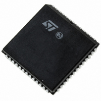
DSM2180F3V-15K6 STMicroelectronics, DSM2180F3V-15K6 Datasheet - Page 11

DSM2180F3V-15K6
Manufacturer Part Number
DSM2180F3V-15K6
Description
IC FLASH 1MBIT 150NS 52PLCC
Manufacturer
STMicroelectronics
Specifications of DSM2180F3V-15K6
Format - Memory
FLASH
Memory Type
FLASH
Memory Size
1M (128K x 8)
Speed
150ns
Interface
Parallel
Voltage - Supply
3 V ~ 3.6 V
Operating Temperature
-40°C ~ 85°C
Package / Case
52-PLCC
Operating Supply Voltage (typ)
3.3V
Operating Supply Voltage (min)
2.97V
Operating Supply Voltage (max)
3.63V
Mounting
Surface Mount
Pin Count
52
Lead Free Status / RoHS Status
Lead free / RoHS Compliant
Other names
497-1336-5
Available stocks
Company
Part Number
Manufacturer
Quantity
Price
Company:
Part Number:
DSM2180F3V-15K6
Manufacturer:
FREESCALE
Quantity:
101
Company:
Part Number:
DSM2180F3V-15K6
Manufacturer:
STMicroelectronics
Quantity:
10 000
TYPICAL CONNECTIONS
Figure 6 shows a typical connection scheme.
Many connection possibilities exist since most
DSM pins are multipurpose. The scheme illustrat-
ed is ideal for a design that needs fast JTAG ISP,
Eight additional general I/O with PLD capability,
access to Flash memory as Byte DMA or as Data
Overlay memory, and the DSP uses Power Down
mode. If your design needs more I/O, or Byte DMA
access to Flash memory is all that is needed (no
Data Overlay), or lowest power consumption is not
an issue, then consider the following options.
Port C JTAG: Figure 6 shows all six JTAG sig-
nals in use full time (not multiplexed with I/0). Us-
ing six-pin JTAG can reduce ISP time by as much
as 30% compared to four-pin JTAG. Alternatively,
four-pin JTAG (TMS, TCK, TDI, TDO) can be used
if more general I/O pins are needed and the few
extra seconds of programming time is not crucial,
freeing up pins PC3 and PC4. Other JTAG options
include mutiplexing JTAG pins with general I/O
(see “Programming In-Circuit using JTAG ISP” on
page 41 and Application Note AN1153) or not us-
ing JTAG at all. If no JTAG is used, the DSM de-
vice has to be programmed on a conventional
programmer before it is installed on the circuit
board. Using no JTAG makes more I/O available.
Pin PD1. If Flash memory will be accessed only
using Byte DMA mode in your design, and no ex-
ternal Data Overlay memory accesses are used,
then pin PD1 can be used for other purposes
(MCUI/O, common CPLD clock input, external
chip select, or PLD input)
Pin PD2. If the DSP will not use Power Down
mode, then PD2 can be used for other purposes
(MCUI/O, external chip select, PLD input)
Pins PC2 and PC7. In Figure 6, these two pins
are used as dedicated address inputs connected
to DSP address outputs. This will route DSP ad-
dress signals A16 and A17 directly into the DPLD.
Be aware that any free pin on Port B, Port C, or
Port D may be used for DSP address inputs, it
does not have to be pins PC2 and PC7.
Pin PB0. This pin is shown as a chip select for an
external peripheral device such as a 16450 or
16550 UART. Equivalently, any free pin on Ports
B, C, or D may be used for this.
DSM2180F3V
11/63


