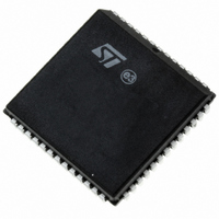
DSM2180F3V-15K6 STMicroelectronics, DSM2180F3V-15K6 Datasheet - Page 41

DSM2180F3V-15K6
Manufacturer Part Number
DSM2180F3V-15K6
Description
IC FLASH 1MBIT 150NS 52PLCC
Manufacturer
STMicroelectronics
Specifications of DSM2180F3V-15K6
Format - Memory
FLASH
Memory Type
FLASH
Memory Size
1M (128K x 8)
Speed
150ns
Interface
Parallel
Voltage - Supply
3 V ~ 3.6 V
Operating Temperature
-40°C ~ 85°C
Package / Case
52-PLCC
Operating Supply Voltage (typ)
3.3V
Operating Supply Voltage (min)
2.97V
Operating Supply Voltage (max)
3.63V
Mounting
Surface Mount
Pin Count
52
Lead Free Status / RoHS Status
Lead free / RoHS Compliant
Other names
497-1336-5
Available stocks
Company
Part Number
Manufacturer
Quantity
Price
Company:
Part Number:
DSM2180F3V-15K6
Manufacturer:
FREESCALE
Quantity:
101
Company:
Part Number:
DSM2180F3V-15K6
Manufacturer:
STMicroelectronics
Quantity:
10 000
Figure 24. Reset (RESET) Timing
Power On Reset, Warm Reset, Power-down
Power On Reset. Upon Power-up, the device re-
quires a Reset (
after V
vice loads internal configurations, clears some of
the registers and sets the Flash memory into Op-
erating mode. After the rising edge of Reset (
SET
additional period, t
cess is allowed.
Table 19. Status During Power-On Reset, Warm Reset and Power-down Mode
Warm Reset. Once the device is up and running,
the device can be reset with a pulse of a much
shorter duration, t
needed before the device is operational after
warm reset. Figure 24 shows the timing of the
Power-up and warm reset.
I/O Pin, Register and PLD Status at Reset. Ta-
ble 19 shows the I/O pin, register and PLD status
during Power On Reset, warm reset and Power-
down mode. PLD outputs are always valid during
warm reset, and they are valid in Power On Reset
once the internal device Configuration bits are
loaded. This loading of the device is completed
typically long before the V
ing level. Once the PLD is active, the state of the
outputs are determined by the PSDsoft Express
equations.
MCU I/O
PLD Output
PMMR0 and PMMR2
OMC Flip-flop status
All other registers
), the device remains in the Reset mode for an
Port Configuration
V
RESET
CC
CC
Register
is steady. During this time period, the de-
RESET
NLNH
OPR
, before the first memory ac-
) pulse of duration t
Power-On Reset
. The same t
V
t NLNH-PO
CC
CC
(min)
Valid after internal PSD
configuration bits are
loaded
Cleared to 0 by internal
Power-On Reset
Cleared to 0
Input mode
Cleared to 0
ramps up to operat-
Power-On Reset
Power-On Reset
OPR
period is
NLNH-PO
t OPR
RE-
Valid
Depends on .re and .pr
equations
Input mode
Unchanged
Cleared to 0
The Flash memory is reset to the Read Array
mode upon Power-up. Sector Select FS0-FS7
must all be Low, Write Strobe (
during Power On Reset for maximum security of
the data contents and to remove the possibility of
a byte being written on the first edge of Write
Strobe (
cle initiation is prevented automatically when V
is below V
Programming In-Circuit using JTAG ISP
In-System Programming (ISP) can be performed
through the JTAG signals on Port C. This serial in-
terface allows programming of the entire DSM de-
vice or subsections (i.e. only Flash memory but not
the PLDs) without and participation of the DSP. A
blank DSM device soldered to a circuit board can
be completely programmed in 10 to 20 seconds.
The basic JTAG signals; TMS, TCK, TDI, and
TDO form the IEEE-1149.1 interface. The DSM
device does not implement the IEEE-1149.1
Boundary Scan functions. The DSM uses the
JTAG interface for ISP only. However, the DSM
device can reside in a standard JTAG chain with
other JTAG devices as it will remain in BYPASS
mode while other devices perform Boundary
Scan.
Warm Reset
Warm Reset
WR
LKO
, CNTL0). Any Flash memory Write cy-
.
Warm Reset
t NLNH-A
t NLNH
Unchanged
Depends on inputs to PLD
(addresses are blocked in
PD mode)
Unchanged
Depends on .re and .pr
equations
Unchanged
Power-down Mode
Power-down Mode
WR
DSM2180F3V
, CNTL0) High,
t OPR
AI02866b
41/63
CC


