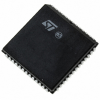
DSM2180F3V-15K6 STMicroelectronics, DSM2180F3V-15K6 Datasheet - Page 34

DSM2180F3V-15K6
Manufacturer Part Number
DSM2180F3V-15K6
Description
IC FLASH 1MBIT 150NS 52PLCC
Manufacturer
STMicroelectronics
Specifications of DSM2180F3V-15K6
Format - Memory
FLASH
Memory Type
FLASH
Memory Size
1M (128K x 8)
Speed
150ns
Interface
Parallel
Voltage - Supply
3 V ~ 3.6 V
Operating Temperature
-40°C ~ 85°C
Package / Case
52-PLCC
Operating Supply Voltage (typ)
3.3V
Operating Supply Voltage (min)
2.97V
Operating Supply Voltage (max)
3.63V
Mounting
Surface Mount
Pin Count
52
Lead Free Status / RoHS Status
Lead free / RoHS Compliant
Other names
497-1336-5
Available stocks
Company
Part Number
Manufacturer
Quantity
Price
Company:
Part Number:
DSM2180F3V-15K6
Manufacturer:
FREESCALE
Quantity:
101
Company:
Part Number:
DSM2180F3V-15K6
Manufacturer:
STMicroelectronics
Quantity:
10 000
DSM2180F3V
port. The three Port Configuration Registers
(PCR), are shown in Table 12. Default is logic 0.
Table 12. Port Configuration Registers (PCR)
Note: 1. See Table 16 for Drive Register bit definition.
Data In Register. The DSP may read the Data In
registers in the csiop block at any time to deter-
mine the logic state of a Port pin. This will be the
state at the pin regardless of whether it is driven by
a source external to the DSM or driven internally
from the DSM device. Reading a logic zero for a bit
in a Data In register means the corresponding Port
pin is also at logic zero. Reading logic one means
the pin is logic one. Each bit in a Data In register
corresponds to an individual Port pin. For a given
Port, bit 0 in a Data In register corresponds to pin
0 of the Port. Example, bit 0 of the Data In register
for Port B corresponds to Port B pin PB0.
Data Out Register. The DSP may write (or read)
the Data Out register in the csiop block at any
time. Writing the Data Out register will change the
logic state of a Port pin only if it is not driven or
controlled by the CPLD. Writing a logic zero to a bit
in a Data Out register will force the corresponding
Port pin to be logic zero. Writing logic one will drive
the pin to logic one. Each bit in the Data Out reg-
isters correspond to Port pins the same way as the
Data In registers described above. When some
pins of a Port are driven by the CPLD, writing to
the corresponding bit in a Data Out register will
have no effect as the CPLD overrides the Data Out
register.
Direction Register. The Direction Register, in
conjunction with the output enable (except for Port
D), controls the direction of data flow in the I/O
Ports. Any bit set to 1 in the Direction Register
causes the corresponding pin to be an output, and
any bit set to 0 causes it to be an input. The default
mode for all port pins is input.
Table 13. Port Pin Direction Control, Output
Enable P.T. Not Defined
34/63
Data In
Data Out
Direction
Drive Select
0
1
Register Name
Direction Register Bit
1
B,C,D
B,C,D
B,C,D
B,C,D
Port
Input
Output
Port Pin Mode
Read
Write/Read
Write/Read
Write/Read
DSP Access
Table 14. Port Pin Direction Control, Output
Enable P.T. Defined
Table 15. Port Direction Assignment Example
Figure 20 and Figure 21 show the Port Architec-
ture diagrams for Ports B and C, respectively. The
direction of data flow for Ports B, and C are con-
trolled not only by the direction register, but also by
the output enable product term from the PLD AND
Array. If the output enable product term is not ac-
tive, the Direction Register has sole control of a
given pin’s direction.
An example of a configuration for a Port with the
three least significant bits set to output and the re-
mainder set to input is shown in Table 15. Since
Port D only contains three pins (shown in Figure
23), the Direction Register for Port D has only the
three least significant bits active.
Drive Select Register. The Drive Select Register
configures the pin driver as Open Drain or CMOS
(standard push/pull) for some port pins, and con-
trols the slew rate for the other port pins. An exter-
nal pull-up resistor should be used for pins
configured as Open Drain. Open Drain outputs are
diode clamped, thus the maximum voltage on an
pin configured as Open Drain is Vcc + 0.7V.
A pin can be configured as Open Drain if its corre-
sponding bit in the Drive Select Register is set to a
1. The default pin drive is CMOS.
Note that the slew rate is a measurement of the
rise and fall times of an output. A higher slew rate
means a faster output response and may create
more electrical noise. A pin operates in a high slew
rate when the corresponding bit in the Drive Reg-
ister is set to 1. The default rate is standard slew.
Table 16 shows the Drive Register for Ports B, C,
and D. It summarizes which pins can be config-
ured as Open Drain outputs and which pins the
slew rate can be set for.
0
0
1
1
0
Bit 7
Register Bit
Direction
0
Bit 6
0
Bit 5
0
1
0
1
Output Enable
0
Bit 4
P.T.
0
Bit 3
1
Bit 2
Input
Output
Output
Output
Port Pin Mode
1
Bit 1
1
Bit 0


