VIPER53ESPTR-E STMicroelectronics, VIPER53ESPTR-E Datasheet - Page 11
VIPER53ESPTR-E
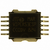
Manufacturer Part Number
VIPER53ESPTR-E
Description
IC OFFLINE SWIT PWM POWERSO10
Manufacturer
STMicroelectronics
Series
VIPER™r
Datasheet
1.VIPER53ESPTR-E.pdf
(31 pages)
Specifications of VIPER53ESPTR-E
Output Isolation
Isolated
Frequency Range
93 ~ 300kHz
Voltage - Input
8.4 ~ 19 V
Voltage - Output
620V
Power (watts)
40W
Operating Temperature
25°C ~ 125°C
Package / Case
PowerSO-10 Exposed Bottom Pad
On Resistance (max)
1.7 Ohms
Supply Voltage (max)
19 V
Supply Voltage (min)
2.6 V
Maximum Operating Temperature
+ 150 C
Minimum Operating Temperature
- 40 C
Mounting Style
SMD/SMT
Number Of Switches
Single
Off Isolation (typ)
8.4 V
Operating Temperature (max)
150C
Operating Temperature (min)
-40C
Pin Count
10
Mounting
Surface Mount
Package Type
PowerSO
Screening Level
Automotive
For Use With
497-8435 - BOARD EVAL FOR VIPER53 28W497-6458 - BOARD EVAL BASED ON VIPER53-E497-6262 - BOARD REF SGL VIPER53 90-264VAC497-5866 - EVAL BOARD 24W NEG OUT VIPER53E497-5865 - EVAL BOARD 24W POS OUT VIPER53E497-4933 - BOARD PWR SUPPLY 24W OUTPUT VIPE
Lead Free Status / RoHS Status
Lead free / RoHS Compliant
Other names
497-5772-2
Available stocks
Company
Part Number
Manufacturer
Quantity
Price
Company:

Part Number:
VIPER53ESPTR-E
Manufacturer:
TI
Quantity:
1 500
Part Number:
VIPER53ESPTR-E
Manufacturer:
ST
Quantity:
20 000


VIPer53EDIP - E / VIPer53ESP - E
7
Standby Mode
The device offers a special feature to address the low load condition. The corresponding
function described hereafter consists of reducing the switching frequency by going into burst
mode, with the following benefits:
For this purpose, a comparator monitores the COMP pin voltage, and maintains the PWM
latch and the Power MOSFET in the Off state as long as V
Block Diagram on page 2). If the output load requires a duty cycle below the one defined by
the minimum turn on of the device, the V
0.5V threshold (V
resumes normal operation as soon as V
regulated in burst mode. The corresponding ripple is not higher than the nominal one at full
load.
In addition, the minimum turn on time which defines the frontier between normal operation
and burst mode changes according to V
time increases to 400ns, whereas for higher voltages, it is 150ns
minimum turn on times resulting from these values are respectively 600 ns and 350 ns,
when taking into account internal propagation time. This brutal change induces an
hysteresis between normal operation and burst mode as shown on
When the output power decreases, the system reaches point 2 where V
V
the effective turn-on time that should be needed at this output power level. Therefore the
regulation loop will quickly drive V
mode and to control the output voltage. The corresponding hysteresis can be seen on the
switching frequency which passes from F
by the components connected to the OSC pin and to FSWstby. Note: This frequency is
actually an equivalent number of switching pulses per second, rather than a fixed switching
frequency since the device is working in burst mode.
As long as the power remains below P
V
missing cycles decreases) as the power approaches P
operation at point 1. The hysteresis cannot be seen on the switching frequency, but it can be
seen in the sudden surge of the COMP pin voltage from point 3 to point 1 at that power
level.
The power points value P
COMPbl
COMPsd
– It reduces the switching losses, thus providing low consumption on the mains lines.
– It allows the regulation of the output voltage, even if the load corresponds to a duty
The device is compliant with “Blue Angel” and other similar standards, requiring less
than 0.5 W of input power when in standby.
cycle that the device is not able to generate because of the internal blanking time,
and associated minimum turn on.
. The minimum turn-on time passes immediately from 350ns to 600ns, exceeding
and the converter works in burst mode. Its “density” increases (i.e. the number of
COMPoff
). The Power MOSFET can be completely Off for some cycles, and
P
RST
P
R ST
STBY
and P
=
1
-- - F
2
=
COMP
1
-- - F
2
STBY
DocRev1
SWnom
RST
to V
SWnom
COMP
COMP
COMP
SWnom
are defined by the following formulas:
the output of the regulation loop remains stuck at
COMPoff
value. Below 1.0V (V
is higher than 0.5V. The output voltage is
net decreases its voltage until it reaches this
tb
which is the normal switching frequency set
Ip
1
+
2
td
V
(Point 3) in order to pass into burst
COMPbl
2
RST
V
COMP
2
and finally resumes normal
IN
Lp
------ -
Lp
1
remains below 0.5V (See
Figure 10 on page 22
COMPbl
Figure 10 on page 22
COMP
), the blanking
Standby Mode
equals
11/31
The
Related parts for VIPER53ESPTR-E
Image
Part Number
Description
Manufacturer
Datasheet
Request
R

Part Number:
Description:
Fixed frequency off line converter
Manufacturer:
STMicroelectronics
Datasheet:

Part Number:
Description:
STATE OF THE ART PRIMARY SIDE SWITCH FOR AC/DC CONVERTERS
Manufacturer:
STMICROELECTRONICS [STMicroelectronics]
Datasheet:
Part Number:
Description:
STMicroelectronics [RIPPLE-CARRY BINARY COUNTER/DIVIDERS]
Manufacturer:
STMicroelectronics
Datasheet:
Part Number:
Description:
STMicroelectronics [LIQUID-CRYSTAL DISPLAY DRIVERS]
Manufacturer:
STMicroelectronics
Datasheet:

Part Number:
Description:
BOARD EVAL FOR MEMS SENSORS
Manufacturer:
STMicroelectronics
Datasheet:
Part Number:
Description:
NPN TRANSISTOR POWER MODULE
Manufacturer:
STMicroelectronics
Datasheet:
Part Number:
Description:
TURBOSWITCH ULTRA-FAST HIGH VOLTAGE DIODE
Manufacturer:
STMicroelectronics
Datasheet:
Part Number:
Description:
Manufacturer:
STMicroelectronics
Datasheet:
Part Number:
Description:
DIODE / SCR MODULE
Manufacturer:
STMicroelectronics
Datasheet:
Part Number:
Description:
DIODE / SCR MODULE
Manufacturer:
STMicroelectronics
Datasheet:
Part Number:
Description:
Search -----> STE16N100
Manufacturer:
STMicroelectronics
Datasheet:
Part Number:
Description:
Search ---> STE53NA50
Manufacturer:
STMicroelectronics
Datasheet: