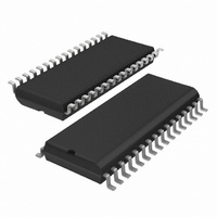
PCA9625D/S911,518 NXP Semiconductors, PCA9625D/S911,518 Datasheet - Page 24

PCA9625D/S911,518
Manufacturer Part Number
PCA9625D/S911,518
Description
IC LED DRIVER RGBA 32-SOIC
Manufacturer
NXP Semiconductors
Type
RGBA LED Driverr
Datasheet
1.PCA9625D512.pdf
(33 pages)
Specifications of PCA9625D/S911,518
Topology
Open Drain, PWM
Number Of Outputs
16
Internal Driver
Yes
Type - Primary
Backlight, LED Blinker
Type - Secondary
RGBA
Frequency
1MHz
Voltage - Supply
2.3 V ~ 5.5 V
Voltage - Output
24V
Mounting Type
Surface Mount
Package / Case
32-SOIC (7.5mm Width)
Operating Temperature
-40°C ~ 85°C
Current - Output / Channel
100mA
Internal Switch(s)
Yes
Lead Free Status / RoHS Status
Lead free / RoHS Compliant
Efficiency
-
Other names
935285147518
PCA9625D/S911-T
PCA9625D/S911-T
PCA9625D/S911-T
PCA9625D/S911-T
NXP Semiconductors
Table 15.
V
[1]
[2]
[3]
14. Dynamic characteristics
Table 16.
[1]
[2]
[3]
PCA9625_2
Product data sheet
Symbol
Address inputs
V
V
I
C
Symbol Parameter
f
t
t
t
t
t
t
t
t
t
t
t
t
t
LI
SCL
BUF
HD;STA
SU;STA
SU;STO
HD;DAT
VD;ACK
VD;DAT
SU;DAT
LOW
HIGH
f
r
SP
DD
IL
IH
i
= 2.3 V to 5.5 V; V
V
V
Each bit must be limited to a maximum of 100 mA and the total package limited to 1600 mA due to internal busing limits.
t
t
A master device must internally provide a hold time of at least 300 ns for the SDA signal (refer to the V
bridge the undefined region of SCL’s falling edge.
VD;ACK
VD;DAT
DD
DD(DRV)FET
must be lowered to 0.2 V in order to reset part.
SCL clock frequency
bus free time between a
STOP and START condition
hold time (repeated) START
condition
set-up time for a repeated
START condition
set-up time for STOP
condition
data hold time
data valid acknowledge time
data valid time
data set-up time
LOW period of the SCL clock
HIGH period of the SCL clock
fall time of both SDA and
SCL signals
rise time of both SDA and
SCL signals
pulse width of spikes that
must be suppressed by the
input filter
= minimum time for SDA data out to be valid following SCL LOW.
= time for Acknowledgement signal from SCL LOW to SDA (out) LOW.
Static characteristics
Dynamic characteristics
and V
Parameter
LOW-level input voltage
HIGH-level input voltage
input leakage current
input capacitance
drv(LED)
SS
= 0 V; T
voltages are independent, but V
amb
…continued
= 40 C to +85 C; unless otherwise specified.
Conditions
Conditions
Rev. 02 — 15 January 2008
drv(LED)
[3][4]
[1]
[2]
[6]
Standard-mode
Min
250
4.7
4.0
4.7
4.0
0.3
0.3
4.7
4.0
V
0
0
-
-
-
DD(DRV)FET
I
2
C-bus
1000
Max
3.45
3.45
100
300
50
16-bit Fm+ I
-
-
-
-
-
-
-
-
at all times.
20 + 0.1C
20 + 0.1C
Fast-mode
Min
100
1.3
0.6
0.6
0.6
0.1
0.1
1.3
0.6
0
0
I
-
Min
0.7V
-
2
0.5
1
C-bus
2
C-bus 100 mA 24 V LED driver
b
b
DD
[5]
[5]
Max
400
300
300
0.9
0.9
50
Typ
-
-
-
3.7
IL
-
-
-
-
-
-
-
-
of the SCL signal) in order to
Plus I
0.26
0.26
0.26
0.05
0.05
0.26
Min
PCA9625
0.5
0.5
50
Fast-mode
0
0
© NXP B.V. 2008. All rights reserved.
-
-
-
Max
+0.3V
5.5
+1
5
2
C-bus
1000
Max
0.45
0.45
120
120
50
DD
-
-
-
-
-
-
-
-
24 of 33
Unit
V
V
pF
Unit
kHz
ns
ns
ns
ns
ns
A
s
s
s
s
s
s
s
s


